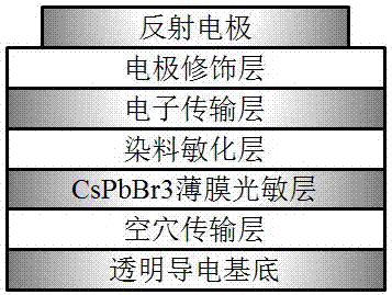
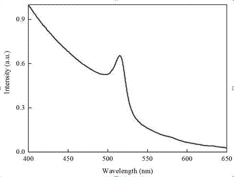
Phthalocyanine dye-sensitized CsPbBr3 photovoltaic cell and manufacturing method thereof
A photovoltaic cell and phthalocyanine dye technology, which is applied in the field of phthalocyanine dye-sensitized CsPbBr3 photovoltaic cells and its manufacturing field, can solve the limitation of CsPbBr3 cell photocurrent and cell energy conversion efficiency, cell short-circuit current, fill factor and open-circuit voltage characteristics Reduce parameters, increase the probability of electron-hole recombination, etc., to achieve the effect of increasing the photoresponse range, good protection, and improving energy conversion efficiency
- Summary
- Abstract
- Description
- Claims
- Application Information
AI Technical Summary
Problems solved by technology
Method used
Image
Examples
Embodiment 1
[0065] A phthalocyanine dye-sensitized CsPbBr3 photovoltaic cell and a manufacturing method thereof, the device structure is Glass / ITO / PEDOT:PSS / CsPbBr3 / SubPc / C60 / Bphen / Al from bottom to top.
[0066] An ITO glass substrate is provided, the ITO thickness is preferably 100-300 nm, the light transmittance is greater than 85%, and the sheet resistance is less than 10 Ω, and the CsPbBr3 photovoltaic cell is made according to the following steps:
[0067] (1) Cleaning of the transparent conductive substrate: The transparent conductive substrate is ultrasonically cleaned with acetone, isopropanol, and deionized water for 20 minutes in sequence, dried with nitrogen and irradiated with a UV lamp for 20 minutes;
[0068] (2) Form a hole transport layer on a transparent conductive substrate: take PEDOT:PSS as a hole transport layer, and deposit it on an ITO transparent conductive substrate by spin coating at a speed of 4000 rpm for 40 s, and then at 120°C Annealing on a heating plate fo...
Embodiment 2
[0086] A phthalocyanine dye-sensitized CsPbBr3 photovoltaic cell and a manufacturing method thereof, the device structure is Glass / ITO / PEDOT:PSS / CsPbBr3 / ClAlPc / PCBM / BCP / Ag from bottom to top.
[0087] Provide any of the above-mentioned ITO glass substrates, the ITO thickness is preferably 100-300 nm, the light transmittance is greater than 85%, and the sheet resistance is less than 10 Ω, and the CsPbBr3 photovoltaic cell is produced according to the following steps:
[0088] (1) Cleaning of transparent conductive substrate: same as embodiment one;
[0089] (2) Forming a hole transport layer on a transparent conductive substrate: same as embodiment one;
[0090] (3) Form a CsPbBr3 thin film photosensitive layer on the hole transport layer, and prepare the CsPbBr3 thin film photosensitive layer according to the following steps:
[0091]A, synthetic CsPbBr polycrystal: with embodiment one;
[0092] B, configuration CsPbBr Precursor solution: with embodiment one;
[0093] C. Sp...
PUM
| Property | Measurement | Unit |
|---|---|---|
| Thickness | aaaaa | aaaaa |
| Thickness | aaaaa | aaaaa |
| Surface root mean square roughness | aaaaa | aaaaa |
Abstract
Description
Claims
Application Information
 - R&D
- Intellectual Property
- Life Sciences
- Materials
- Tech Scout
- Unparalleled Data Quality
- Higher Quality Content
- 60% Fewer Hallucinations
Browse by: Latest US Patents, China's latest patents, Technical Efficacy Thesaurus, Application Domain, Technology Topic, Popular Technical Reports.
© 2025 PatSnap. All rights reserved.Legal|Privacy policy|Modern Slavery Act Transparency Statement|Sitemap|About US| Contact US: help@patsnap.com


