
Array substrate, display panel, display device and manufacturing method of array substrate

A technology for array substrates and manufacturing methods, which is applied in the fields of array substrates, the manufacture of array substrates, display devices, and display panels, and can solve the problems of too many masks and increased manufacturing costs, and achieve the effects of reducing manufacturing costs and reducing quantities

Active Publication Date: 2017-08-25
SHANGHAI AVIC OPTOELECTRONICS
View PDF5 Cites 21 Cited by
  • Summary
  • Abstract
  • Description
  • Claims
  • Application Information

AI Technical Summary

Problems solved by technology

[0004] Obviously, using the above method, the number of mask plates required is large, which increases the manufacturing cost

Method used


Image

  • Array substrate, display panel, display device and manufacturing method of array substrate
  • Array substrate, display panel, display device and manufacturing method of array substrate
  • Array substrate, display panel, display device and manufacturing method of array substrate

Examples


Embodiment Construction

[0105] The present application will be described in further detail below through specific embodiments and in conjunction with the accompanying drawings.

[0106] It should be noted that the orientation words such as "up", "down", "left", and "right" described in the embodiments of the present application are described from the angles shown in the drawings, and should not be interpreted as limiting the implementation of the present application. Example limitations. Furthermore, in this context, it also needs to be understood that when it is mentioned that an element is formed "on" or "under" another element, it can not only be directly formed "on" or "under" another element, but also be formed "on" or "under" another element. An element may be formed "on" or "under" another element indirectly through intervening elements.

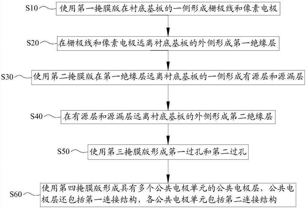
[0107] Please combine figure 1 , figure 1 It is a flow chart of the manufacturing method of the array substrate provided in this application. An embodim...


PUM


Abstract

The invention relates to the technical field of display, and particularly relates to an array substrate, a display panel, a display device and a manufacturing method of the array substrate. The manufacturing method comprises the steps of manufacturing grid lines and pixel electrodes by adopting a first mask plate, manufacturing a thin film transistor and a touch signal line by adopting a second mask plate, manufacturing a first via hole and a second via hole by adopting a third mask plate, and manufacturing a common electrode layer by adopting a fourth mask plate, wherein the common electrode layer comprises a first connecting structure and a common electrode unit, the common electrode unit comprises a second connecting structure, the first connecting structure is contacted with a drain electrode and the pixel electrodes through the first via hole, and the second connecting structure is contacted with the touch signal line through the second via hole. According to the invention, manufacturing of the array substrate is realized through the four mask plates, the number of the mask plates is reduced, and thus the manufacturing cost can be reduced.

Description

technical field [0001] The present invention relates to the field of display technology, in particular to an array substrate, a display panel, a display device and a method for manufacturing the array substrate. Background technique [0002] With the continuous development of liquid crystal display technology, liquid crystal display panels are widely used in display devices such as mobile terminals, household televisions, digital cameras, and computers. The liquid crystal display panel includes an array substrate, a color filter substrate, and liquid crystals located between the array substrate and the packaging substrate. [0003] The built-in touch liquid crystal display integrates the touch electrodes that realize the touch function on the array substrate or the color film substrate. Among them, when the touch electrodes are integrated on the array substrate, the array substrate includes pixel electrodes, gate lines, active layer, source and drain layers, touch signal li...

Claims


Application Information

Patent Timeline
Patent Type & Authority Applications(China)
IPC IPC(8): H01L21/84H01L27/12G02F1/1362G06F3/041
CPCG02F1/136227G02F1/136286G06F3/041G06F2203/04103G02F1/136231G02F1/136295H01L27/124H01L27/1288
Inventor 金慧俊朱雪婧曹兆铿
Owner SHANGHAI AVIC OPTOELECTRONICS
Learn More