
Light-emitting device with beam shaping structure and manufacturing method of light-emitting device

A light-emitting device and structure adjustment technology, which is applied to electrical components, electric solid-state devices, circuits, etc., can solve the problems of complicated manufacturing process, increased production cost, and decreased luminous efficiency of the package, and achieve simple manufacturing process, reduced loss, and increased luminous angle Effect

Active Publication Date: 2017-08-15
MAVEN OPTRONICS CO LTD
View PDF8 Cites 7 Cited by
  • Summary
  • Abstract
  • Description
  • Claims
  • Application Information

AI Technical Summary

Problems solved by technology

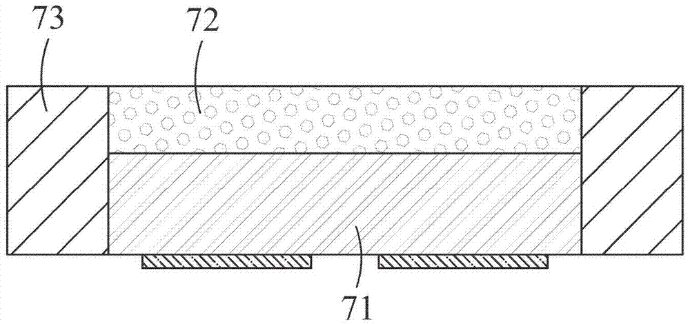
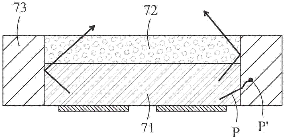
However, if Figure 1C As shown, the reflective structure 73 of the top-emitting CSP light-emitting device is formed by mixing high-concentration light-scattering particles in polymer materials. Usually, the weight percentage concentration of light-scattering particles needs to be greater than 30% to achieve light The effect of reflection, but some photons (such as path P) will be excessively lost (dissipation) in the reflective structure 73, for example, photons are absorbed at P' (the end of the photon path) in the reflective structure 73, so it is caused by photon loss. Reduce the luminous efficiency of the package; and, in the production, another process is required to cover the four facades of the LED chip with reflective materials, which makes the process more complicated; if it is necessary to further use a precision mold (mold) for more accurate When controlling the manufacturing process of the reflective structure, it will also significantly increase the production cost

Method used


Image

  • Light-emitting device with beam shaping structure and manufacturing method of light-emitting device
  • Light-emitting device with beam shaping structure and manufacturing method of light-emitting device
  • Light-emitting device with beam shaping structure and manufacturing method of light-emitting device

Examples


Embodiment Construction

[0070] see Figure 2A and 2B As shown, it is a perspective view and a full cross-sectional view of a light emitting device 1A according to a first preferred embodiment of the present invention. The light emitting device 1A may include an LED chip 10, a fluorescent structure 20, a beamshaping structure (or BSS for short) 30 and a light-transmitting structure 40, and the fluorescent structure 20, the BSS 30 and the light-transmitting structure 40 A light-transmitting packaging structure 200 can also be formed; the technical content of the multiple components will be described in sequence as follows.

[0071] The LED chip 10 is a flip-chip LED chip, which includes an upper surface 11 , a lower surface 12 , a vertical surface 13 and an electrode group 14 . The upper surface 11 and the lower surface 12 are oppositely disposed, and the vertical surface 13 is formed between the upper surface 11 and the lower surface 12 and connects the upper surface 11 and the lower surface 12 . I...


PUM


Abstract

The invention discloses a chip scale packaging light-emitting device and a manufacturing method thereof. The light-emitting device comprises a flip chip type LED chip and a beam shaping structure to form a single-color light-emitting device, and the light-emitting device can also comprise a fluorescent structure arranged on the LED chip to form a white light-emitting device. The beam shaping device disclosed by the structure is formed by mixing optical scattering particles with a high polymer material and is arranged at a side part of the light-emitting device or at an upper part of the light-emitting device, and the weight percent of the optical scattering particles is not larger than 30%. Therefore, the transfer paths of a part of light beams can be changed by the beam shaping structure due to optical scattering characteristic, the light rays emitted in a lateral direction can be reduced when the beam shaping structure is arranged at the side part of the light-emitting device, the light rays emitted in a positive direction can be reduced when the beam shaping structure is arranged at the upper part of the light-emitting device, and thus, the beam shape and the light-emitting angle of the light-emitting device can be adjusted.

Description

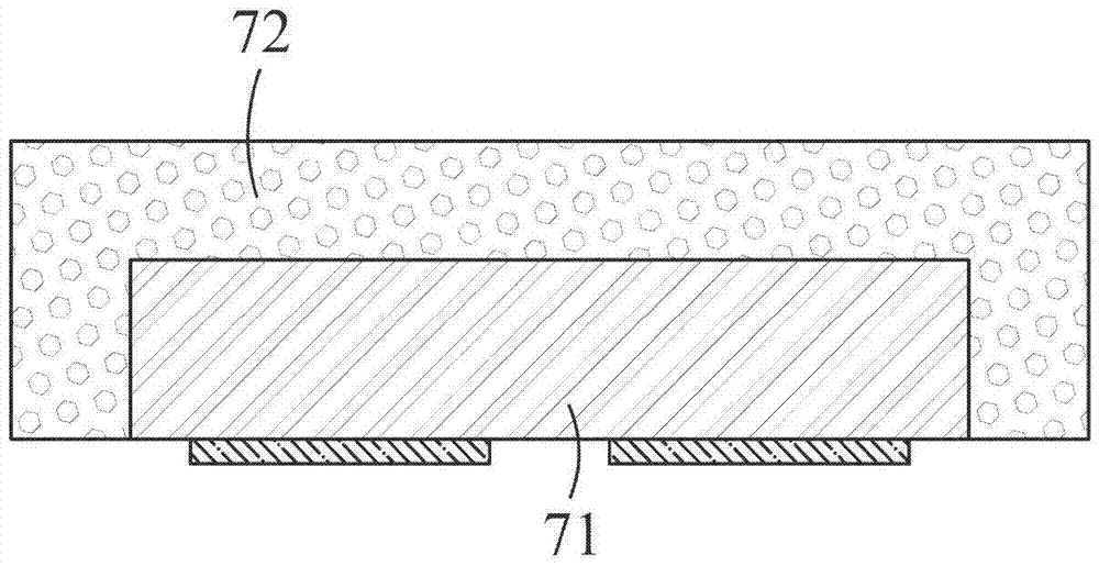
[0001] 【Technical field】 [0002] The present invention relates to a light-emitting device and a manufacturing method thereof, in particular to a chip-level packaging light-emitting device with a light shape adjustment structure and a manufacturing method thereof. [0003] 【Background technique】 [0004] With the evolution of LED technology, chip scale packaging (chip scale packaging, CSP) light-emitting devices have begun to receive a lot of attention in recent years due to their obvious advantages. Taking the most widely used white light CSP light-emitting device as an example, such as Figure 1A As shown, the white light CSP light-emitting device disclosed in the prior art is composed of a flip-chip LED chip 71 and a fluorescent structure 72 covering the LED chip. The fluorescent structure 72 covers the upper surface and four vertical surfaces of the LED chip 71. , so the CSP light-emitting device can emit light from its top surface and four sides, that is, emit light from f...

Claims


Application Information

Patent Timeline
IPC IPC(8): H01L33/58H01L33/50H01L33/48H01L25/075
CPCH01L25/0753H01L33/48H01L33/50H01L33/58H01L2224/96
Inventor 陈杰王琮玺
Owner MAVEN OPTRONICS CO LTD
Learn More