Method for generating metal coatings in controllable regions of surface of probe of atomic force microscope
A technology of atomic force microscope and metal coating, which is applied in the direction of metal material coating process, coating, liquid chemical plating, etc., can solve the problems of poor reproducibility, rough coating, high cost, etc., and achieve low cost, dense film layer, heavy weight high performance
- Summary
- Abstract
- Description
- Claims
- Application Information
AI Technical Summary
Problems solved by technology
Method used
Image
Examples
Embodiment 1
[0067] 1. The preparation of the high molecular polymer film containing hydrogen fluoride: poly(2-vinylpyridine) is selected as the high molecular polymer, and toluene is selected as the organic solution.
[0068] (1a) Surface treatment of silicon wafer: take and cut into 20×20mm 2 Silicon wafers of different sizes were ultrasonically washed three times with acetone, ethanol, and ultrapure water, each time for at least 5 minutes; The volume ratio of hydrogen is 7:3), soaking at 80-100°C for 30 minutes; finally washing with ultrapure water, N 2 Just blow dry;
[0069] (1b) Preparation of high molecular polymer film containing hydrogen fluoride: Add 10 mg / mL poly(2-vinylpyridine) toluene solution dropwise on the surface-treated silicon wafer, heat treatment at 60°C to obtain poly(2 -vinylpyridine) film, then dropwise add 1wt% HF solution drop by drop on the surface of the film, and let it stand in the air, after it dries, it will form a polymeric polymer containing hydrogen fl...
Embodiment 2
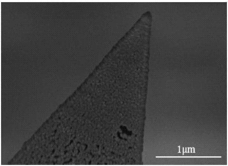
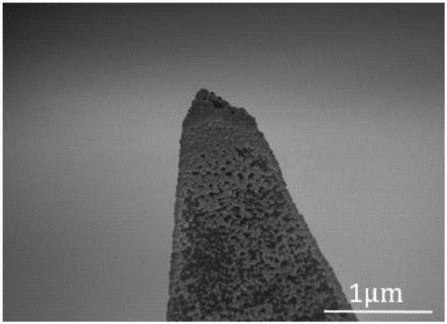
[0077] The specific experimental operation is as shown in Example 1, the only difference is that the depth of the probe tip piercing into the hydrogen fluoride film in step 2 is less than or equal to 2 μm.
[0078] figure 2 The SEM image of the metal coating at the activation site on the surface of the AFM probe tip prepared in Example 2 of the present invention. Depend on figure 2 It can be seen that the gold tip coating formed by the reaction on the surface of the AFM probe tip is about 16nm, and the tip radius of the tip is about 15nm. The gold tip coating is a uniform and dense coating of gold nanoparticles.
Embodiment 3
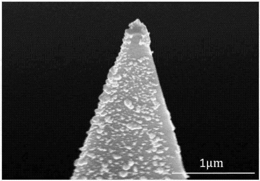
[0080] The specific experimental operation is as shown in Example 1, the only difference is that the depth of the probe tip piercing into the hydrogen fluoride film in step 2 is less than or equal to 3 μm; the reaction time in step 3 is 1 min, and the gold content is 0.1 mmol / L.
[0081] image 3 The SEM image of the metal coating at the activation site on the surface of the AFM probe tip prepared in Example 3 of the present invention. Depend on image 3 It can be seen that the gold tip coating formed by the reaction on the surface of the AFM probe tip is about 12nm, and the tip radius of the tip is about 10nm. The gold tip coating is a uniform and dense coating of gold nanoparticles.
PUM
| Property | Measurement | Unit |
|---|---|---|
| Radius | aaaaa | aaaaa |
| Depth | aaaaa | aaaaa |
| Radius | aaaaa | aaaaa |
Abstract
Description
Claims
Application Information
 - Generate Ideas
- Intellectual Property
- Life Sciences
- Materials
- Tech Scout
- Unparalleled Data Quality
- Higher Quality Content
- 60% Fewer Hallucinations
Browse by: Latest US Patents, China's latest patents, Technical Efficacy Thesaurus, Application Domain, Technology Topic, Popular Technical Reports.
© 2025 PatSnap. All rights reserved.Legal|Privacy policy|Modern Slavery Act Transparency Statement|Sitemap|About US| Contact US: help@patsnap.com


