
Method for manufacturing semiconductor device

A manufacturing method, semiconductor technology, applied in the direction of semiconductor devices, semiconductor/solid-state device manufacturing, chemical instruments and methods, etc., can solve unproven, problems with epitaxial growth layers, and epitaxial layer defects are not suitable for advanced semiconductor devices and circuit problems

Active Publication Date: 2017-08-08
TAIWAN SEMICON MFG CO LTD
View PDF9 Cites 0 Cited by
  • Summary
  • Abstract
  • Description
  • Claims
  • Application Information

AI Technical Summary

Problems solved by technology

However, in at least some known processes, the number and / or size of epitaxial layer defects left after epitaxial layer growth (eg, formed during epitaxial layer growth) may not be suitable for use in advanced semiconductor devices and circuit fabrication
In some instances, non-uniformity of epitaxially grown layers can also be problematic for device and / or circuit fabrication
[0004] Therefore, known techniques have not been proven to be completely satisfactory in all respects

Method used


Image

  • Method for manufacturing semiconductor device
  • Method for manufacturing semiconductor device
  • Method for manufacturing semiconductor device

Examples


Embodiment Construction

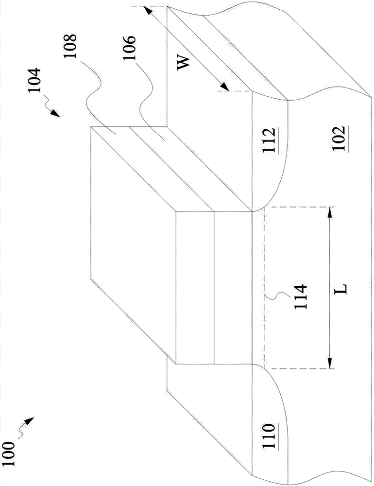
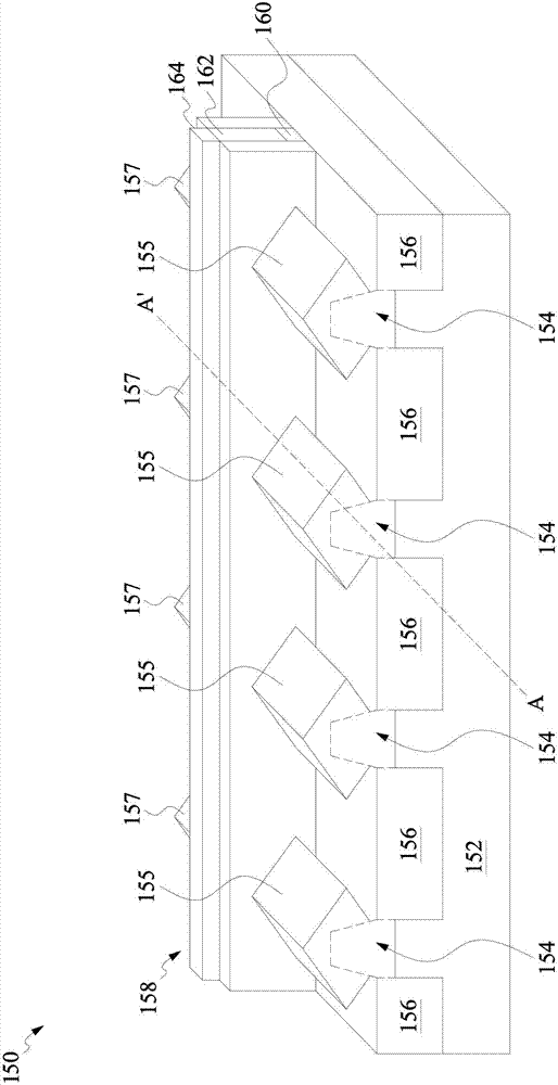
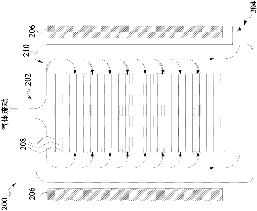
[0026] The following invention provides many different embodiments, or illustrations, to implement different features of the provided subject matter. Specific illustrations of components and arrangements described below are for the purpose of simplifying the present invention. These are of course only examples and are not intended to be limiting. For example, the description that the first feature is formed on or above the second feature includes the embodiment that the first feature and the second feature are in direct contact, and also includes that other features are formed between the first feature and the second feature, An embodiment such that the first feature and the second feature are not in direct contact. In addition, the present invention repeats element symbols and / or letters in various illustrations. This repetition is for simplicity and clarity and does not imply any relationship between the various embodiments and / or configurations discussed.

[0027] Furthe...


PUM

PropertyMeasurementUnit
sizeaaaaaaaaaa
sizeaaaaaaaaaa

Abstract

The invention discloses a method for manufacturing a semiconductor device. A method and structure for providing a two-step defect reduction bake, followed by a high-temperature epitaxial layer growth. In various embodiments, a semiconductor wafer is loaded into a processing chamber. While the semiconductor wafer is loaded within the processing chamber, a first pre-epitaxial layer deposition baking process is performed at a first pressure and first temperature. In some cases, after the first pre-epitaxial layer deposition baking process, a second pre-epitaxial layer deposition baking process is then performed at a second pressure and second temperature. In some embodiments, the second pressure is different than the first pressure. By way of example, after the second pre-epitaxial layer deposition baking process and while at a growth temperature, a precursor gas may then be introduced into the processing chamber to deposit an epitaxial layer over the semiconductor wafer.

Description

technical field [0001] The present invention relates to a manufacturing method of a semiconductor device, in particular to an epitaxial growth method and its structure. Background technique [0002] The electronics industry has gone through a period of increasing demand for smaller and faster electronic devices that can simultaneously support a large number of ever-increasing complex and complex functions. Accordingly, in the semiconductor industry, there is a continuing trend to manufacture low cost, high performance and low power integrated circuits. To date, most of these goals have been achieved by reducing the size of semiconductor integrated circuits (ie, minimizing feature size), thereby improving production efficiency and reducing associated costs. However, this scaling also adds complexity to the semiconductor manufacturing process. Accordingly, to achieve continued advances in semiconductor integrated circuits and devices, similar advances in semiconductor manufa...

Claims


Application Information

Patent Timeline
Patent Type & Authority Applications(China)
IPC IPC(8): H01L21/02
CPCH01L21/02255H01L21/02293H01L21/02656H01L21/02576H01L21/02579H01L21/02661C23C16/0218C30B25/186C30B29/06C23C16/4408H01L29/66795H01L29/785H01L29/7848H01L29/66772H01L21/02532H01L21/0262H01L29/167H01L29/66568H01L21/823431H01L29/42392
Inventor 上野哲嗣游明华杨建伦
Owner TAIWAN SEMICON MFG CO LTD
Learn More