An asymmetric annular microelectrode phase-change memory unit and device
A phase-change memory and ring-shaped electrode technology, which is applied in the direction of electrical components, electric solid-state devices, semiconductor devices, etc., can solve problems such as increased power consumption, heat dissipation, and minimum size restrictions, so as to reduce write power consumption and improve Storage density, effect of reducing operating current
- Summary
- Abstract
- Description
- Claims
- Application Information
AI Technical Summary
Problems solved by technology
Method used
Image
Examples
Embodiment 1
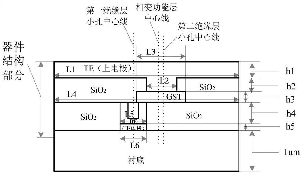
[0061] In this embodiment, the longitudinal cross-sectional structure diagram of the phase-change memory cell with asymmetric annular electrodes designed by three-dimensional thermal simulation is as follows: Figure 4 As shown, the top view of the interface between the phase change material and the lower electrode is as follows Figure 5 As shown, the longitudinal cross-sectional structure diagram of a common electrode phase-change memory cell is shown in image 3 shown. Discuss the influence of the asymmetric ring electrode structure and the common T-shaped electrode structure on the reset current. The shape of the whole asymmetric annular electrode phase-change memory unit is a cuboid; the small holes of the first insulating layer, the small holes of the second insulating layer and the phase-change material are all cylinders. Figure 4 Among them, h5 is the thickness of the lower electrode layer, h4 is the thickness of the hole of the ring electrode in the first insulatin...
Embodiment 2
[0067] This embodiment discusses the influence of the offset s between the centerline of the phase change functional layer and the centerline of the first insulating layer on the reset current in the asymmetrical ring-shaped electrode structure. The longitudinal cross-sectional structure of the designed asymmetric ring electrode phase-change memory cell is shown in Figure 10shown. For the convenience of analysis, the centerline of the aperture of the second insulating layer coincides with the centerline of the phase-change functional layer, that is, the offset t and The offset s between the centerline of the phase change functional layer and the centerline of the small hole in the first insulating layer is equal. The thickness of the lower electrode layer is h5=10nm, the thickness of the ring-shaped electrode hole in the first insulating layer is h4=100nm, the radius of the insulating material filled in the center of the ring-shaped electrode hole is r=6nm, and the thickness...
Embodiment 3
[0070] This embodiment discusses the influence of the offset t between the centerline of the second insulating layer and the centerline of the first insulating layer on the reset current in the asymmetric ring electrode structure. The longitudinal cross-sectional structure of the designed asymmetric ring electrode phase-change memory cell is shown in Figure 12 shown. The offset s=15nm between the centerline of the phase-change functional layer and the centerline of the small hole of the first insulating layer, the thickness of the lower electrode layer is h5=10nm, and the thickness of the small hole of the annular electrode in the first insulating layer is h4=100nm, The radius of the insulating material filled in the center of the annular electrode aperture is r=6nm, the thickness of the upper electrode hole is h2=10nm, the thickness of the upper electrode layer is h1=10nm, the diameter of the phase change functional layer is L3=30nm, and the characteristic size L2= L6 = 30n...
PUM
| Property | Measurement | Unit |
|---|---|---|
| thickness | aaaaa | aaaaa |
| width | aaaaa | aaaaa |
| thickness | aaaaa | aaaaa |
Abstract
Description
Claims
Application Information
 - Generate Ideas
- Intellectual Property
- Life Sciences
- Materials
- Tech Scout
- Unparalleled Data Quality
- Higher Quality Content
- 60% Fewer Hallucinations
Browse by: Latest US Patents, China's latest patents, Technical Efficacy Thesaurus, Application Domain, Technology Topic, Popular Technical Reports.
© 2025 PatSnap. All rights reserved.Legal|Privacy policy|Modern Slavery Act Transparency Statement|Sitemap|About US| Contact US: help@patsnap.com


