Array substrate and manufacturing method thereof

A technology of an array substrate and a manufacturing method, which is applied in the field of liquid crystal displays, can solve the problems of low efficiency and complicated manufacturing process of the array substrate, and achieve the effects of reducing the yellow light manufacturing process, improving the production efficiency and saving the cost.

Active Publication Date: 2019-09-27
TCL CHINA STAR OPTOELECTRONICS TECH CO LTD
View PDF4 Cites 0 Cited by
  • Summary
  • Abstract
  • Description
  • Claims
  • Application Information

AI Technical Summary

Problems solved by technology

[0004] The invention provides an array substrate and a manufacturing method thereof, which are used to solve the technical problems of complicated manufacturing process and low efficiency of the array substrate in the prior art

Method used


Image

  • Array substrate and manufacturing method thereof
  • Array substrate and manufacturing method thereof
  • Array substrate and manufacturing method thereof

Examples


Embodiment 1

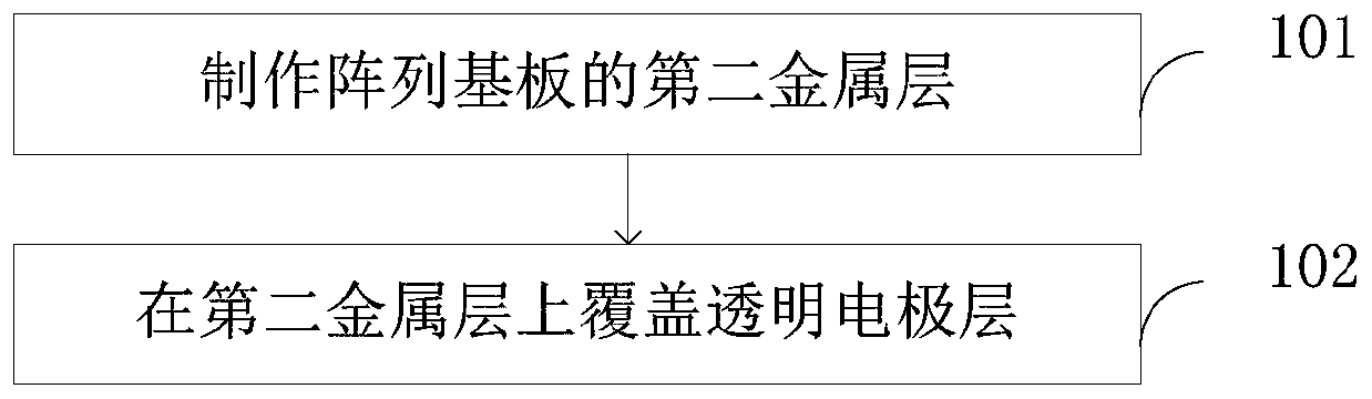
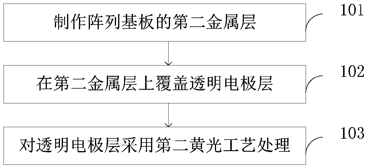
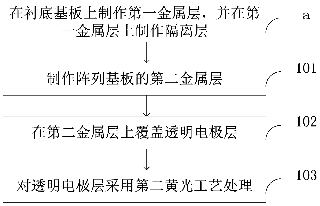
[0029] Such as figure 1 As shown, Embodiment 1 of the present invention provides a method for manufacturing an array substrate, including:

[0030] In step 101, a second metal layer of the array substrate is fabricated, and the second metal layer is formed by a metal thin film layer treated by a first yellow light process. In the semiconductor industry, silicon wafers or metal thin films are coated, soft-baked, exposed, developed, and hard-baked to make certain patterns. This process is called yellow light, which is one of the fine circuit manufacturing processes. Specifically, the yellow light process (including the first yellow light process and the second yellow light process hereinafter) is a process of processing the metal thin film layer to include at least one pattern, and the specific steps include coating a photoresist on the metal thin film layer, Then use the first mask to expose the photoresist, then use the developer to wash away the photoresist to be etched, and...

Embodiment 2

[0040] An embodiment of the present invention provides an array substrate, including: a second metal layer and a transparent electrode layer directly covering the second metal layer, wherein the second metal layer is formed by a metal thin film layer treated by a first yellow light process.

[0041] Further, the pattern of the second mask 2 used when the transparent electrode layer is subjected to the second yellow light process includes the pattern of the first mask 1 used when the metal thin film layer is subjected to the first yellow light process. Such as Figure 4 , Figure 5 as shown, Figure 4 is the pattern of the first mask plate 1, Figure 5 It is the pattern of the second mask plate 2, which includes the pattern of the first mask plate 1 (the pattern of the first mask plate 1 is composed of the unetched part of the second metal layer), so that When the transparent electrode layer is etched, the second metal layer will not be damaged.

[0042] Furthermore, in ano...


PUM


Abstract

The invention provides an array substrate and a manufacturing method thereof. The method comprises steps: a second metal layer of the array substrate is manufactured, wherein a metal thin film layer is processed through a first yellow light process to form the second metal layer; and the second metal layer is covered with a transparent electrode layer. According to the above array substrate manufacturing method and the array substrate, the transparent electrode layer is directly manufactured on the second metal layer of the array substrate, conduction is realized through direct contact between the second metal layer and the transparent electrode layer, manufacturing of a via hole in a passivation layer in the prior art is reduced, a yellow light process is reduced, the cost is saved, and the production efficiency is improved.

Description

technical field [0001] The invention relates to the technical field of liquid crystal displays, in particular to an array substrate and a manufacturing method thereof. Background technique [0002] Polymer Stabilized Vertically Aligned (Polmer Stabilized Vertically Aligned, PSVA for short) liquid crystal is a new type of liquid crystal display technology. In the traditional PSVA design, the main film layer of the array substrate needs 5 times of yellow light process, which are M1 (ie, the first metal layer), AS (amorphous silicon), M2 (ie, the second metal layer), PV (passivation layer) and ITO, wherein a via hole is provided on the PV layer for conducting M2 and ITO. [0003] In the above-mentioned traditional PSVA design, the manufacturing process of the array substrate has many passes, the manufacturing process is complicated, and the efficiency is low. Therefore, a new method is urgently needed to improve the above-mentioned process. Contents of the invention [0004...

Claims


Application Information

Patent Timeline
Patent Type & Authority Patents(China)
IPC IPC(8): H01L21/77H01L27/12
Inventor 邓竹明
Owner TCL CHINA STAR OPTOELECTRONICS TECH CO LTD
Why Eureka
Try Eureka