Epitaxial wafer of gallium nitride-based light-emitting diode and preparation method thereof
A light-emitting diode, gallium nitride-based technology, applied in semiconductor devices, electrical components, circuits, etc., can solve the problem of reducing the luminous efficiency of light-emitting diodes, and achieve the effect of improving the ability of composite light emission, shortening the transmission distance, and improving the luminous efficiency.
- Summary
- Abstract
- Description
- Claims
- Application Information
AI Technical Summary
Problems solved by technology
Method used
Image
Examples
Embodiment 1
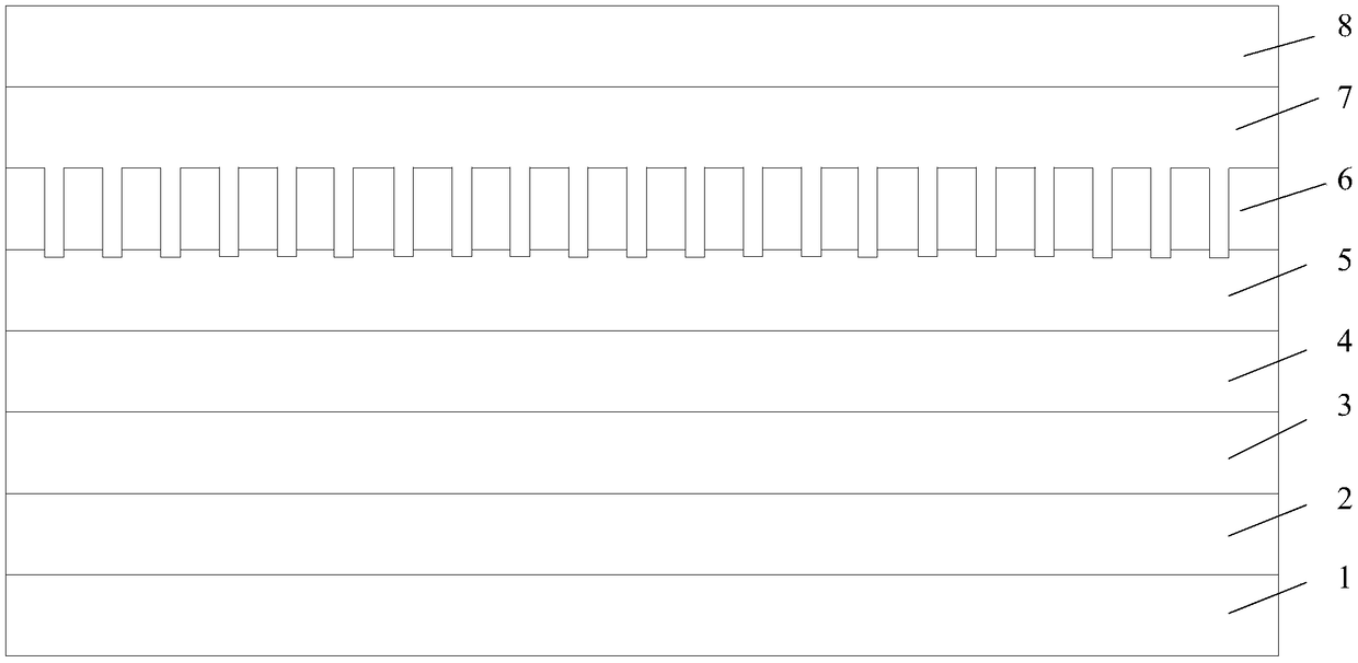
[0035] An embodiment of the present invention provides an epitaxial wafer of a gallium nitride-based light-emitting diode, see figure 1 , the epitaxial wafer includes a sapphire substrate 1, and a GaN buffer layer 2, an undoped GaN layer 3, an N-type GaN layer 4, a multi-quantum well layer 5, a P-type AlGaN layer 6, P-type GaN layer 7 .
[0036] In this embodiment, the multi-quantum well layer is formed by sequentially stacking a plurality of sub-layers, and each sub-layer includes a quantum well layer and a quantum barrier layer stacked on the quantum well layer. like figure 2 As shown, there are several through holes in the P-type AlGaN layer 6 and the quantum barrier layer 51 closest to the P-type AlGaN layer. The quantum well layer 52 of the AlGaN layer, and the P-type GaN layer 7 are filled in the through hole.
[0037] Optionally, the cross-section of the through hole perpendicular to the stacking direction of the epitaxial wafers may be square, circular, star-shaped...
Embodiment 2
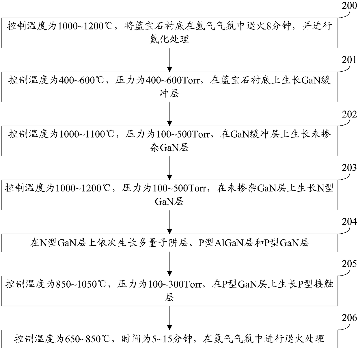
[0053] An embodiment of the present invention provides a method for preparing an epitaxial wafer of a gallium nitride-based light-emitting diode, which is suitable for preparing the epitaxial wafer provided in Embodiment 1. See image 3 , the preparation method comprises:
[0054] Step 200: Control the temperature to 1000-1200° C., anneal the sapphire substrate in a hydrogen atmosphere for 8 minutes, and perform nitriding treatment.
[0055] Understandably, step 200 can clean the surface of the sapphire substrate.
[0056] In this embodiment, the sapphire substrate 1 adopts (0001) crystal orientation sapphire.
[0057] Step 201: Control the temperature to 400-600° C. and the pressure to 400-600 Torr to grow a GaN buffer layer on the sapphire substrate.
[0058] Optionally, the thickness of the GaN buffer layer may be 15-35 nm.
[0059] Optionally, after step 201, the preparation method may further include:
[0060] The control temperature is 1000-1200° C., the pressure is ...
PUM
 Abstract
Description
Claims
Application Information
 - R&D
- Intellectual Property
- Life Sciences
- Materials
- Tech Scout
- Unparalleled Data Quality
- Higher Quality Content
- 60% Fewer Hallucinations
Browse by: Latest US Patents, China's latest patents, Technical Efficacy Thesaurus, Application Domain, Technology Topic, Popular Technical Reports.
© 2025 PatSnap. All rights reserved.Legal|Privacy policy|Modern Slavery Act Transparency Statement|Sitemap|About US| Contact US: help@patsnap.com


