Manufacturing method of a membrane key switch and a membrane key panel

A manufacturing method and key technology, which are applied in the direction of electrical switches, crosstalk/noise/electromagnetic interference reduction (, printed circuit components, etc.) , shielding problems and other problems, to achieve the effect of ensuring electromagnetic shielding effect, high conductivity, and avoiding misoperation

Inactive Publication Date: 2019-02-26
中山市川广电子科技有限公司
View PDF6 Cites 0 Cited by
  • Summary
  • Abstract
  • Description
  • Claims
  • Application Information

AI Technical Summary

Problems solved by technology

[0002] Membrane key switches are used as operation panels in many electronic products today. While bringing convenient operation and elegant appearance, they also encounter problems of electromagnetic shielding and electrostatic interference: on the one hand, because the membrane key switch itself has a large The shielding of electronic products brings a lot of problems. On the other hand, the circuit and components of the switch part are easily disturbed by radio frequency and static electricity, resulting in misoperation of the operation. Therefore, it is particularly important to solve the shielding problem.

Method used


Image

  • Manufacturing method of a membrane key switch and a membrane key panel
  • Manufacturing method of a membrane key switch and a membrane key panel
  • Manufacturing method of a membrane key switch and a membrane key panel

Examples


Embodiment 1

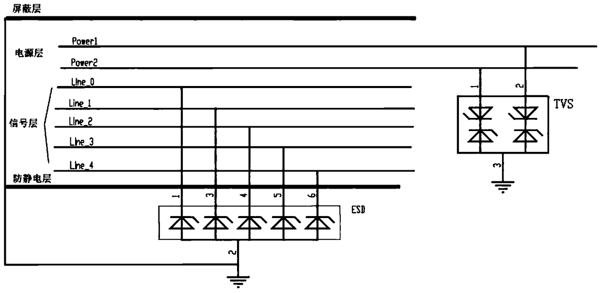
[0048] See figure 1 and figure 2 , a membrane key switch of this embodiment is composed of a printed circuit board 1 and a membrane key panel 2 covered on the printed circuit board 1; the printed circuit board 1 is sequentially composed of a ground layer 11, a power layer 12 and several Signal Layer 13. The thin film key panel 2 is as follows from top to bottom: a first protective layer 21, an antistatic layer 22, a PET substrate 23, a pattern layer 24, a shielding layer 25, a second protective layer 26, a conductive adhesive layer 27 and a key cushion layer 28; A transparent window 29 is set on the first protective layer 21, antistatic layer 22, PET substrate 23, pattern layer 24, shielding layer 25, second protective layer 26 and conductive adhesive layer 27; antistatic layer 22, PET substrate 23, Pattern layer 24, shielding layer 25, second protective layer 26 and conductive adhesive layer 27 are provided with at least one process via 210, and antistatic layer 22, shield...


PUM


Abstract

The invention discloses a membrane key switch and a manufacturing method of a membrane key panel. The membrane key switch is composed of a printed circuit board and the membrane key panel covering the printed circuit board. The printed circuit board comprises a ground wire layer, a power layer and a plurality of signal layers in sequence from bottom to top. A TVS power protector is connected between the ground wire layer and the power layer. An ESD static electricity resistor is connected between the ground wire layer and the multiple signal layers. The membrane key panel sequentially comprises a first protection layer, an antistatic layer, a PET substrate, a pattern layer, a shielding layer, a second protection layer, a conducive adhesive layer and a button cushion layer from top to bottom; the ground wire layer of the printed circuit board is connected with the shielding layer and the antistatic layer of the membrane key panel. The TVS power protector is connected between the power layer and the ground wire layer so as to reduce instantly-generated electromagnetic interference, and the ESD static electricity resistor is connected between the signal lines and the ground wire, so that the static electricity phenomenon generated by the touch effect is reduced, and a switch membrane switch body is protected.

Description

technical field [0001] The invention relates to a manufacturing method of a membrane key switch and a membrane key panel. Background technique [0002] Membrane key switches are used as operation panels in many electronic products today. While bringing convenient operation and elegant appearance, they also encounter problems of electromagnetic shielding and electrostatic interference: on the one hand, because the membrane key switch itself has a large The shielding of electronic products brings great problems. On the other hand, the circuit and components of the switch part are easily disturbed by radio frequency and static electricity, resulting in misoperation of operation. Therefore, it is particularly important to solve the shielding problem. Contents of the invention [0003] The first object of the present invention is to provide a membrane key switch. [0004] The technical solution for achieving the first purpose of the present invention is a membrane key switch, ...

Claims


Application Information

Patent Timeline
Patent Type & Authority Patents(China)
IPC IPC(8): H01H13/14H01H13/02H01H11/00H05K1/02
CPCH01H11/00H01H13/02H01H13/14H05K1/0216H05K1/0218H05K1/0259
Inventor 黄宇航宋和明俞克非
Owner 中山市川广电子科技有限公司
Why Eureka
Try Eureka