A sealing device and sealing method for an interface between a microenvironment and a wafer box

A technology of sealing device and wafer box, which is applied in the direction of transportation and packaging, electrical components, conveyor objects, etc. It can solve the problems of poor positioning accuracy, limited adjustment ability, and low reliability, so as to achieve good transmission reliability and ensure stability performance, to ensure the effect of cleanliness

Active Publication Date: 2020-02-21
BEIJING NAURA MICROELECTRONICS EQUIP CO LTD
View PDF4 Cites 0 Cited by
  • Summary
  • Abstract
  • Description
  • Claims
  • Application Information

AI Technical Summary

Problems solved by technology

[0007] The industry is working hard to completely solve the above-mentioned sealing problems, and some of them use a wafer box pressing device or other locking devices at the bottom of the wafer box to prevent the position accuracy of the wafer box from changing, but the positioning accuracy of these mechanisms is still poor, and the adjustment ability limited and less reliable

Method used


Image

  • A sealing device and sealing method for an interface between a microenvironment and a wafer box
  • A sealing device and sealing method for an interface between a microenvironment and a wafer box
  • A sealing device and sealing method for an interface between a microenvironment and a wafer box

Examples


Embodiment Construction

[0039] The specific embodiment of the present invention will be further described in detail below in conjunction with the accompanying drawings.

[0040] It should be noted that, in the following specific embodiments, when describing the embodiments of the present invention in detail, in order to clearly show the structure of the present invention for the convenience of description, the structures in the drawings are not drawn according to the general scale, and are drawn Partial magnification, deformation and simplification are included, therefore, it should be avoided to be interpreted as a limitation of the present invention.

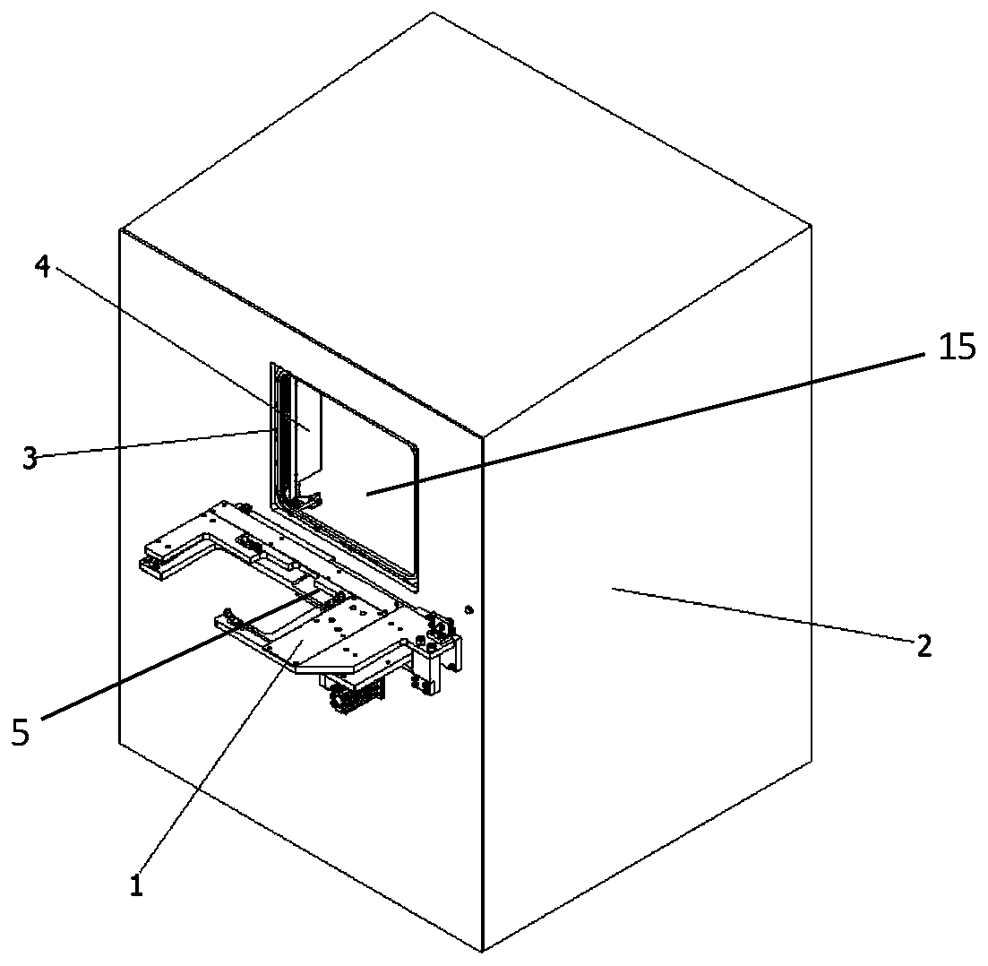
[0041] In the following specific embodiments of the present invention, please refer to figure 1 , figure 1 It is a schematic diagram of the interface state between the microenvironment and the wafer box. Such as figure 1 As shown, a sealing device for the interface between the microenvironment and the wafer box of the present invention is arranged...


PUM


Abstract

The invention discloses a microenvironment and wafer box interface sealing device comprising the following units: a frame type seal ring fixed plate sealed and stacked on one side, facing to the wafer box, of the interface; a frame type seal ring support plate stacked outside the seal ring fixed plate in an adjustable manner; a frame type seal ring fixed on the frame type seal ring support plate so as to at least surround and cover partial the inner and outer side walls of the support plate; when the wafer box moves to the interface and compacts the seal ring support plate, the seal ring support plate can form elastic deformations, so the seal ring on two sides of the seal ring support plate can form deformations corresponding to the compressions, thus sealing the wafer box with the seal ring support plate, sealing seal ring support plate with the seal ring fixed plate, and effectively sealing the interface. The invention also correspondingly discloses a sealing method.

Description

technical field [0001] The invention relates to the field of semiconductor process equipment, more specifically, to a sealing device and a sealing method for an interface between a microenvironment and a wafer box. Background technique [0002] In the semiconductor process equipment, the wafer is transported into the reaction chamber through the wafer box for processing, and then the wafer is sent back to the wafer box after the process is completed, so it is inevitable to open the wafer box door and process the wafer in it. Pick and place. During the wafer picking and placing process, the exposed area of ​​the wafer needs to control the low oxygen content, and the exposed area is usually a relatively closed space, and the closed space is filled with nitrogen or other inert gases to ensure low oxygen content. oxygen content. This confined space is often referred to as a microenvironment. [0003] To ensure a low oxygen content in the microenvironment, good sealing and iso...

Claims


Application Information

Patent Timeline
Patent Type & Authority Patents(China)
IPC IPC(8): H01L21/67H01L21/68H01L21/677
CPCH01L21/67011H01L21/67126H01L21/67739H01L21/68
Inventor 徐冬刘东
Owner BEIJING NAURA MICROELECTRONICS EQUIP CO LTD
Why Eureka
Try Eureka