Array substrate and liquid crystal panel provided with same

An array substrate and polysilicon technology, applied in optics, instruments, electrical components, etc., can solve the problems of limited overlapping area, breakdown of the gate insulating layer, damage to the pixel function of the display area, etc., to improve yield, improve electrostatic protection, Avoid the effect of damage

Inactive Publication Date: 2017-05-31
WUHAN CHINA STAR OPTOELECTRONICS TECH CO LTD
View PDF6 Cites 11 Cited by
  • Summary
  • Abstract
  • Description
  • Claims
  • Application Information

AI Technical Summary

Problems solved by technology

During the manufacturing process of the array substrate, before the ESD high voltage generated by the driving circuit area 7' is transmitted to the display area 6' along the gate line 3', the gate line 3' only passes through the polysilicon in the dummy pixel area 1'. Line 4' overlaps twice on different planes, (only about 100 nanometer thick gate insulating layer is separated between gate line 3' and polysilicon wiring 4', between gate line 3' and polysilicon wiring 4' The high voltage difference easily causes the gate insulating layer to be broken down), and the overlapping area is very limited, so the ESD high voltage that has not been released often continues to pass into the display area 6' and causes the pixels in the display area 6' to be damaged. Abnormal bright or dark spots caused by the 6' edge of the display area
[0005] In other words, the inventors of the present application found that when the overlapping area of ​​the polysilicon wiring 4' and the gate line 3' in the dummy pixel area 1' is equal to or smaller than that of the polysilicon wiring 4' and the gate line in the display area 6' When the line 3' overlaps the area, the static voltage cannot be effectively released
Therefore, when the electrostatic voltage is too large, the dummy pixel area cannot fully release it, causing the electrostatic voltage to continue to pass into the display area along the gate line, destroying the pixel function of the display area

Method used


Image

  • Array substrate and liquid crystal panel provided with same
  • Array substrate and liquid crystal panel provided with same
  • Array substrate and liquid crystal panel provided with same

Examples


Embodiment Construction

[0026] The present invention will be further described below in conjunction with accompanying drawing.

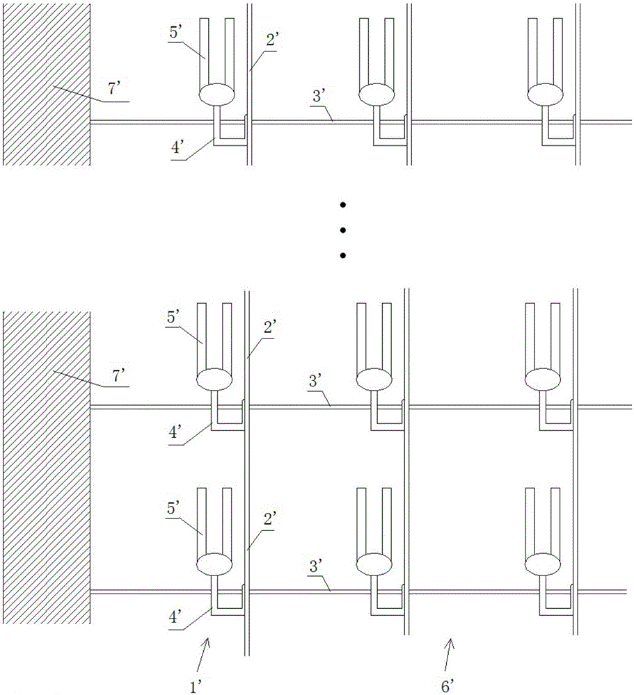
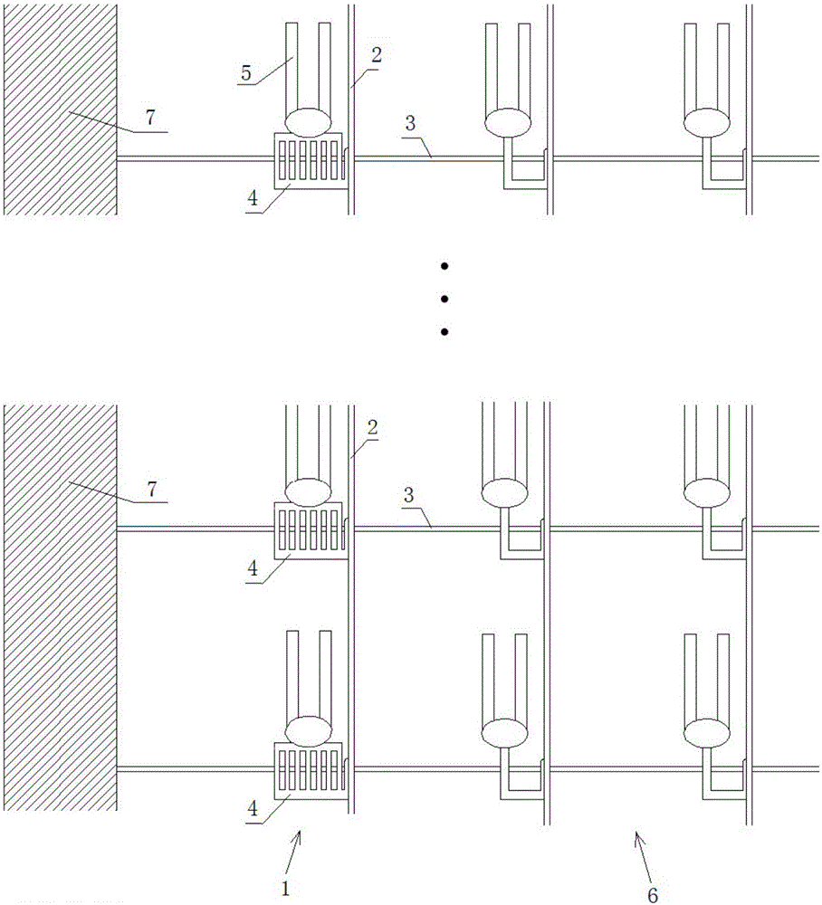
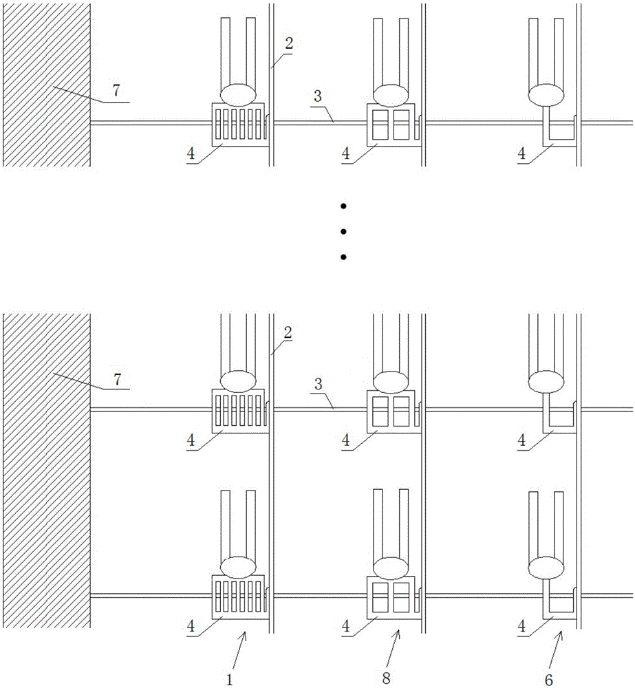
[0027] Such as figure 2 As shown in , it is a partial schematic diagram of a preferred embodiment of the array substrate according to the present invention. The array substrate mainly includes: a dummy pixel area 1 , a source line 2 , a gate line 3 , a polysilicon line 4 , a pixel ITO line 5 , a display area 6 and a driving circuit area 7 . Wherein, the dummy pixel area 1 is located at the edge of the display area 6 , that is, between the display area 6 and the driving circuit area 7 . Both the display area 6 and the dummy pixel area 1 are provided with a source line 2, a gate line 3, a polysilicon line 4, and a pixel ITO line 5, the source line 2 is perpendicular to the gate line 3, and the polysilicon line The lines 4 cross the gate lines 3 on different planes, and the polysilicon lines 4 and the source lines 2 are connected through via holes (not shown in the figure)....


PUM


Abstract

The invention provides an array substrate and a liquid crystal panel provided with the same. The array substrate comprises a virtual pixel area, a display area and a drive circuit area, wherein the virtual pixel area is located between the display area and the drive circuit area; polycrystalline silicon lines and gate lines which are intercrossed at different planes are arranged in the display area and the virtual pixel area, wherein the noncoplanar overlapped area of the polycrystalline silicon lines and the gate lines in the virtual pixel area is larger than thatof the polycrystalline silicon lines and the gate lines in the display area. The array substrate can release static voltage effectively and greatly reduce static voltage which is probably transmitted to the display area along the gate lines and prevents damage to the pixel function of the display area.

Description

technical field [0001] The invention belongs to the field of electrical protection, and in particular relates to an array substrate capable of effectively releasing static voltage and a liquid crystal panel with the array substrate. Background technique [0002] During the manufacturing process of liquid crystal panel devices or when working within a certain range of voltage, current and power consumption, a large number of accumulated static charges will generate high-voltage discharge when the conditions are suitable, and electrostatic discharge (ESD, Elctro-Static Discharge) passes through the circuit device The instantaneous high voltage transmission of the lead may cause the breakdown of the insulation layer of the circuit device, resulting in the loss of the function of the circuit device. When low temperature polysilicon (LTPS, Low Temperature Poly-Silicon) technology is applied to the display panel, due to the introduction of TFT modules, digital signals have to work...

Claims


Application Information

Patent Timeline
Patent Type & Authority Applications(China)
IPC IPC(8): H01L27/02H01L27/12G02F1/1362
CPCG02F1/136204G02F1/136286G02F2202/22H01L27/0251H01L27/124G02F2202/104G02F1/136295H01L27/0288H01L27/0296H01L29/78696H01L27/1244
Inventor 虞晓江
Owner WUHAN CHINA STAR OPTOELECTRONICS TECH CO LTD
Why Eureka
Try Eureka