An electron beam high-precision high-frequency deflection scanning device

A deflection scanning, high-precision technology, applied to electrode devices and related components, improving energy efficiency, improving process efficiency, etc., can solve the problems of small electron beam deflection angle, slow electron beam scanning speed, and small driving current, etc. Improve deflection scanning speed, large-scale deflection scanning, and uniform electromagnetic field distribution

Active Publication Date: 2018-06-15
BEIHANG UNIV
View PDF10 Cites 0 Cited by
  • Summary
  • Abstract
  • Description
  • Claims
  • Application Information

AI Technical Summary

Problems solved by technology

[0003] In the prior art, deflection scan coils are mostly ring-shaped. The magnetic field directions of the inner and outer sides of such coil windings are opposite to the center of the coil, and the parallelism of the magnetic induction lines is poor, resulting in low magnetic induction intensity, poor magnetic field uniformity, and electron beam deflection angles. Small, generally only used for small swings of the electron beam near the molten pool during welding, it is difficult to achieve precise control of deflection scanning and meet the requirements of large-area scanning in electron beam rapid manufacturing
On the other hand, the existing deflection scan coil adopts a magnetic core structure, so that the inductance of the deflection scan coil is relatively large, thus causing the deflection scan frequency of the coil to be mostly low; moreover, the drive circuit of the existing deflection scan coil is generally A low-voltage operational amplifier is used for current amplification, the driving voltage is low, the driving current is small, and the changing speed of the driving current is slow, which makes the scanning speed of the electron beam slow, and it is easy to leave scanning traces during the scanning process, which is not conducive to the processing of precision parts.

Method used


Image

  • An electron beam high-precision high-frequency deflection scanning device
  • An electron beam high-precision high-frequency deflection scanning device
  • An electron beam high-precision high-frequency deflection scanning device

Examples


Embodiment Construction

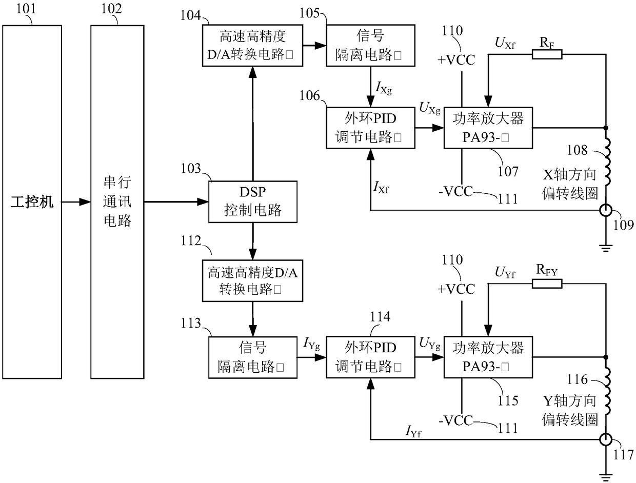
[0085] The invention provides an electron beam high-precision high-frequency deflection scanning device, and its specific implementation method is:

[0086] The electron beam high-precision high-frequency deflection scanning device includes:

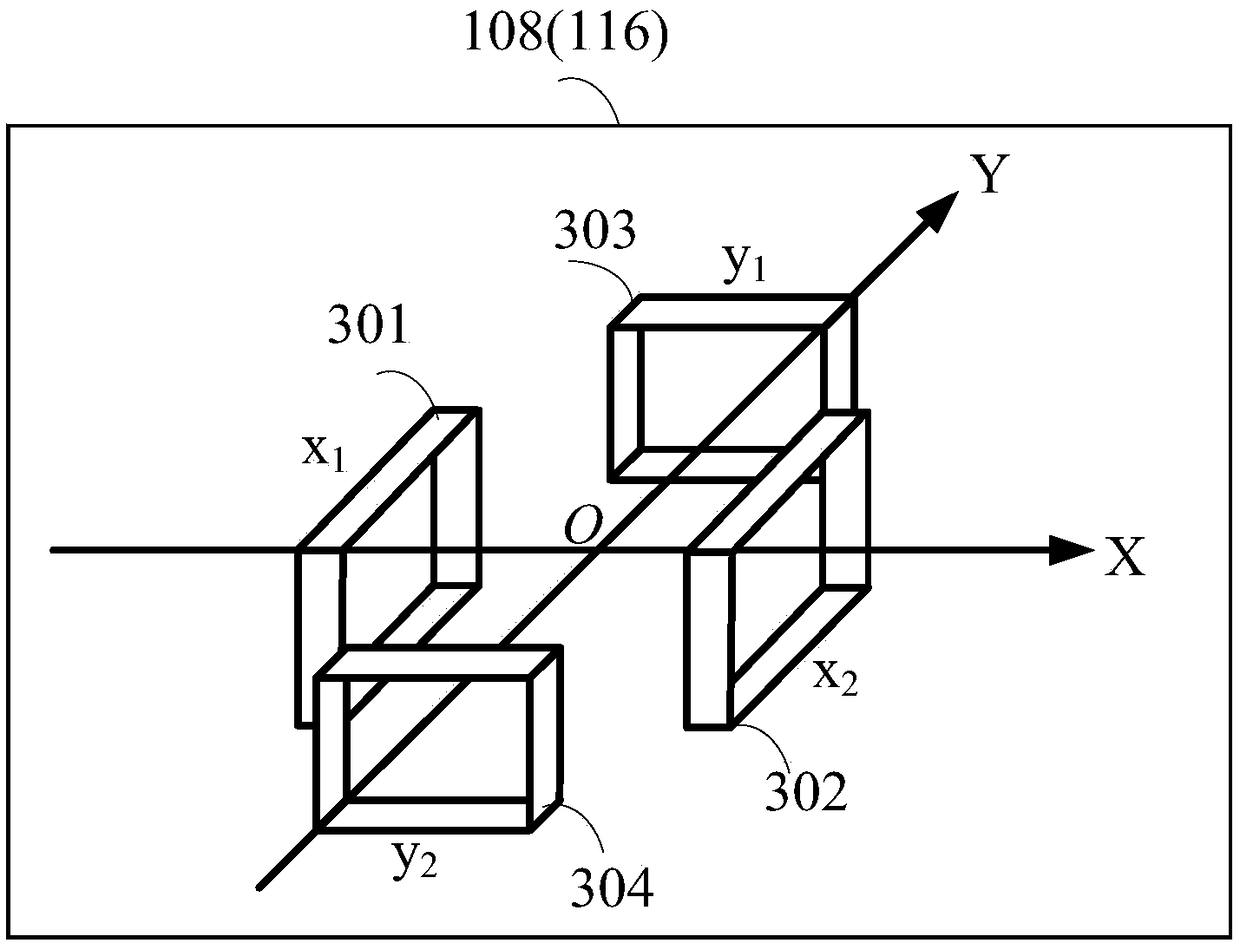
[0087] see figure 1 As shown, industrial computer 101, serial communication circuit 102, DSP control circuit 103, high-speed and high-precision D / A conversion circuit Ⅰ 104, high-speed and high-precision D / A conversion circuit Ⅱ 112, signal isolation circuit Ⅰ 105, signal isolation circuit Ⅱ 113, outer ring PID regulation circuit Ⅰ106, outer ring PID regulation circuit Ⅱ114, power amplifier PA93-Ⅰ107, power amplifier PA93-Ⅱ115, X-axis direction deflection scanning coil 108, current sensor Ⅰ109, Y-axis direction deflection scanning coil 116, current sensor Ⅱ117, +160V DC voltage source 110 and -160V DC voltage source 111. The position connection relationship between them is: the industrial computer 101 is connected to the DSP control ci...


PUM


Abstract

An electron beam high-precision high-frequency deflection scanning device, including digital signal processing, that is, DSP control circuit, power amplifier PA93, deflection scanning coil, etc.; the DSP control circuit generates two voltage signals through a high-speed high-precision D / A conversion circuit, and then passes through After the signal isolation circuit, the scanning current waveforms of the deflection scanning coils in the X-axis and Y-axis directions are respectively given; at the same time, the coil currents in the X-axis and Y-axis directions are respectively collected as feedback of the scanning current waveform; then, the scanning current setting and feedback The signal is then input to the outer ring PID adjustment circuit and the inner ring power amplifier PA93 in the X-axis and Y-axis directions respectively, and the amplified signal drives the deflection scanning coil to generate an electromagnetic field to deflect and scan the electron beam. The invention not only improves the control precision of the electron beam deflection scanning, but also realizes the high-frequency change of the coil driving current, thereby increasing the deflection scanning speed and realizing the high-speed, high-precision and wide-range deflection scanning of the electron beam.

Description

technical field [0001] The invention provides an electron beam deflection and scanning device, in particular an electron beam high-precision and high-frequency deflection scanning device, which belongs to the technical field of electron beam processing. Background technique [0002] Electron beam rapid manufacturing technology has the advantages of high deposition efficiency and good forming quality. It can realize efficient, rapid and near-net shape manufacturing of complex structural parts. It has a very broad application prospect in the manufacture of complex structural parts in aerospace and medical fields. According to the different filling materials, electron beam rapid manufacturing can be divided into two types: electron beam selective melting (powder spreading) and electron beam fuse deposition (wire feeding). Electron beam selective melting uses electron beam high-frequency deflection to scan surface heat sources to realize substrate preheating, powder preheating, ...

Claims


Application Information

Patent Timeline
Patent Type & Authority Patents(China)
IPC IPC(8): H01J29/76
CPCB22F10/10B22F10/00B22F12/49B22F12/90B22F10/20Y02P10/25
Inventor 张伟朱起超李平林付航
Owner BEIHANG UNIV
Why Eureka
Try Eureka