


Quick Research
Generate reliable direction feasibility study reports for your R&D in just a few steps.

Technical Q&A
Discover and master advanced knowledge NOW. Basics, ideas, possibilities, all at once.

Find Solutions
As an expert in R&D theories, this can generate solutions to your technical problems instantly.

Evaluate Feasibility
Analyze your overall solution with one click, know your potential R&D risks in advance.

Monitor Landscape
Get weekly tech updates, stay abreast of the latest tech innovations and key insights.
Image display device manufacturing method, hardening resin composition used therein, and image display device
An image display device and curable resin technology, applied in nonlinear optics, optics, instruments, etc., can solve problems such as visibility problems, liquid crystal cell gap changes, and ripples
- Summary
- Abstract
- Description
- Claims
- Application Information
AI Technical Summary
Problems solved by technology
Method used
Image

Examples
no. 1 approach
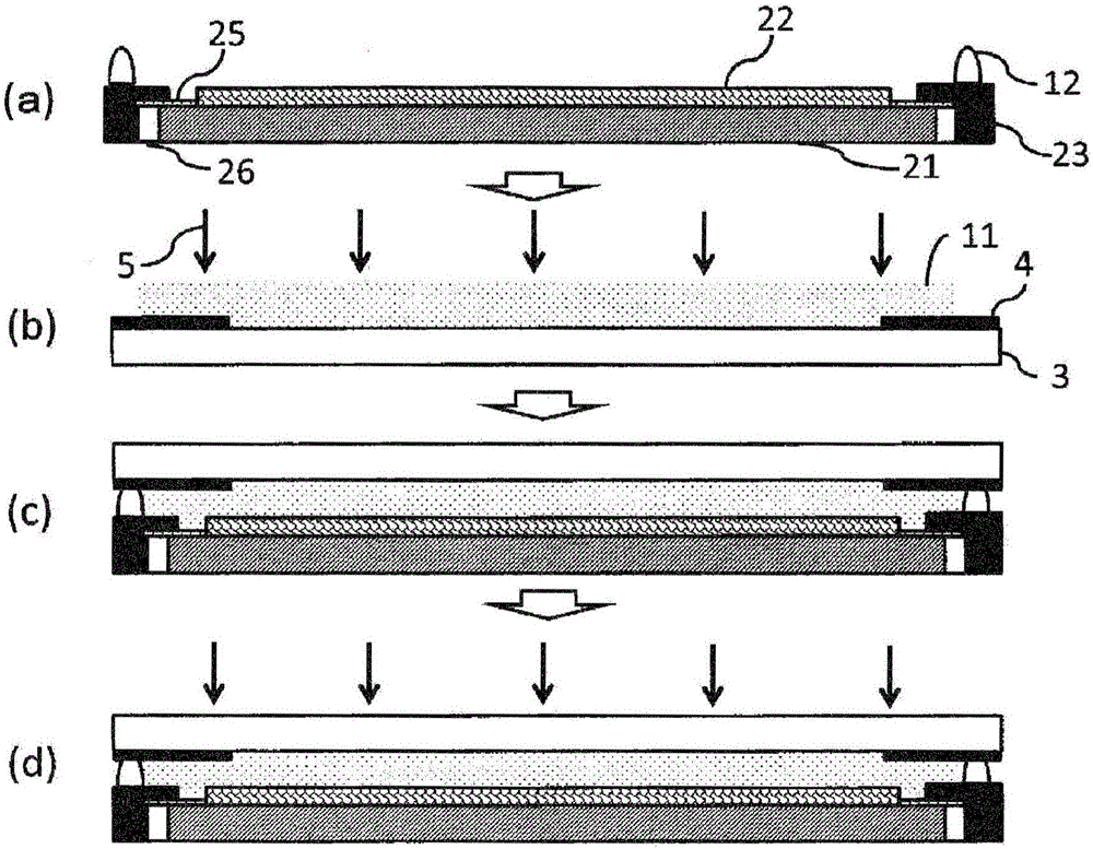
[0056] figure 1 It is a process drawing which shows 1st Embodiment of the manufacturing process of the optical member of this invention.
[0057] This method is a method of obtaining an optical member (image display device) by bonding the liquid crystal display unit 1 and the protective plate 2 together.
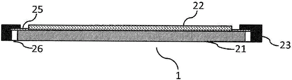
[0058] The liquid crystal display unit 1 is a liquid crystal display unit in which a liquid crystal material is sealed between a pair of substrates on which electrodes are formed, and includes a polarizing plate, a driving circuit, a signal input cable, and a backlight unit.
[0059] figure 2 It is a cross-sectional view showing a main part of an example of the liquid crystal display unit 1 . Such as figure 2 As shown, this liquid crystal display unit 1 has a configuration in which a polarizing plate 22 is disposed on a liquid crystal display cell 21 , and a sealing body 23 is disposed on the liquid crystal display cell 21 so as to surround the polarizing plate 22 . He...
no. 2 approach
[0155] The optical member of the present invention can also be produced by the second embodiment modified as follows from the first embodiment.
[0156] [Process A]
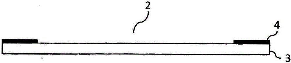
[0157] First, if Figure 5 As shown in (a), the 2nd curable resin composition 12 containing a (meth)acrylate (A) and a photoinitiator (B) is apply|coated on the surface on the guard plate 2 in which the light shielding part 4 was formed.
[0158] [Process B]
[0159] Then, if Figure 5 As shown in (b), the first curable resin composition 11 is coated on the surface of the protective plate 2 on which the light-shielding portion 4 is formed, and then the obtained coating film is irradiated with ultraviolet rays 5 to obtain The cured product layer exists in the cured portion on the lower side of the layer (the transparent substrate side viewed from the curable resin composition) and the uncured portion on the upper side of the coating layer (opposite to the transparent substrate side).
[0160] At this time, when ...
no. 3 approach
[0168] The optical member of the present invention can also be produced by the third embodiment modified as follows on the basis of the first embodiment and the second embodiment.
[0169] [Process A]
[0170] First, if Image 6 As shown in (a), the second curable resin composition 12 containing (meth)acrylate (A) and photopolymerization initiator (B) is coated on the display surface of the liquid crystal display unit 1 and the protective plate 2. On the surface of the face of the light shielding part 4 .
[0171] [Process B]
[0172] Then, if Image 6 As shown in (b), the first curable resin composition 11 containing (meth)acrylate (A) and photopolymerization initiator (B) is coated on the display surface of the liquid crystal display unit 1 and the protective plate 2. On the surface of the face of the light shielding part 4 .
[0173] The obtained coating film was irradiated with ultraviolet rays 5 to obtain a cured portion existing on the lower side of the coating film...
PUM
| Property | Measurement | Unit |
|---|---|---|
| Viscosity | aaaaa | aaaaa |
| Thickness | aaaaa | aaaaa |
| Viscosity | aaaaa | aaaaa |
Abstract
Description
Claims
Application Information
 - R&D Engineer
- R&D Manager
- IP Professional
- Industry Leading Data Capabilities
- Powerful AI technology
- Patent DNA Extraction
Browse by: Latest US Patents, China's latest patents, Technical Efficacy Thesaurus, Application Domain, Technology Topic, Popular Technical Reports.
© 2024 PatSnap. All rights reserved.Legal|Privacy policy|Modern Slavery Act Transparency Statement|Sitemap|About US| Contact US: help@patsnap.com