
Flash memory structure and manufacturing method thereof

A manufacturing method and flash memory technology, which are applied to semiconductor devices, electrical components, circuits, etc., can solve problems such as reducing the performance of flash memory structures and adverse effects of gate structures, and achieve the effects of avoiding adverse effects, improving competitiveness, and improving performance.

Active Publication Date: 2017-05-10
WUHAN XINXIN SEMICON MFG CO LTD
View PDF5 Cites 3 Cited by
  • Summary
  • Abstract
  • Description
  • Claims
  • Application Information

AI Technical Summary

Problems solved by technology

[0003] However, the source electrode manufacturing method of the traditional flash memory structure is to use a self-aligned source (SAS) method to define the region of the source electrode with a photomask, etch, and ion implantation to form the source electrode after forming the gate structure. This method will cause some adverse effects on the gate structure, thereby reducing the performance of the entire flash memory structure

Method used


Image

  • Flash memory structure and manufacturing method thereof
  • Flash memory structure and manufacturing method thereof
  • Flash memory structure and manufacturing method thereof

Examples


Embodiment Construction

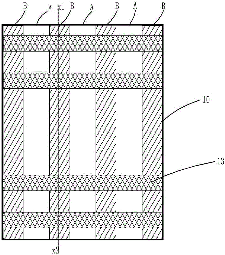
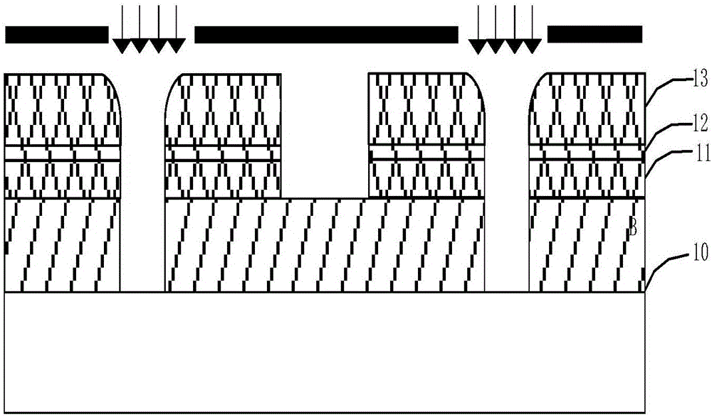
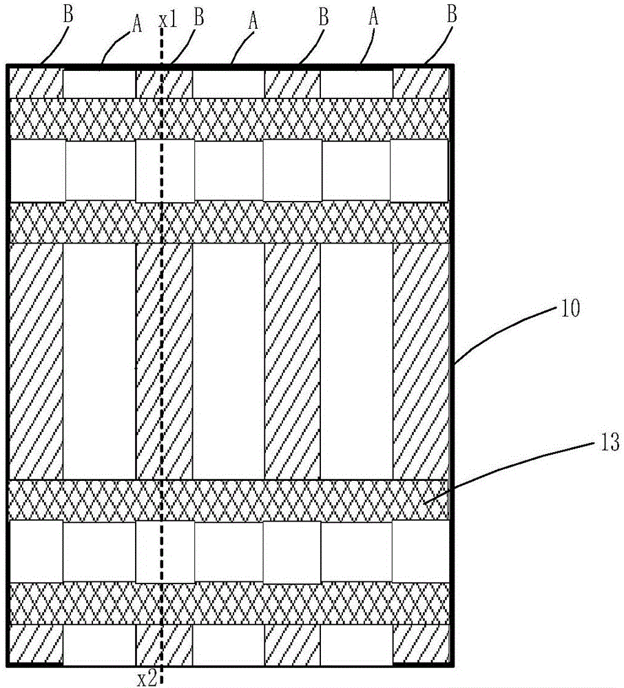
[0036] see Figure 1 to Figure 5 , is a top view and a cross-sectional structure diagram of a conventional flash memory structure manufacturing method well known to the inventor, and the flash memory structure manufacturing method includes: providing a substrate 10; forming an active region A and a shallow flash memory structure in the substrate 10 Trench isolation structure (STI) B, the active regions A are isolated by the shallow trench isolation structure B, and the shallow trench isolation structure B is filled with silicon dioxide; then, in the A gate structure is formed on the substrate 10, and the gate structure includes a floating gate layer 11 deposited on the substrate 10, a control gate layer 13 stacked on the floating gate layer 11, and a control gate layer on the control gate layer. 13 and the floating gate layer 11 is provided with an ONO (oxide-nitride-oxide) layer 12, such as figure 1 and 2 Shown; Next, adopt self-aligned source process (SAS) to form source 1...


PUM


Abstract

The invention discloses a flash memory structure and a manufacturing method thereof. Active areas are defined in a substrate, the active areas comprise a first active area and a second active area, and the first active area and the second active area are mutually vertically distributed; a gate structure is formed on the substrate, the gate structure is positioned on two parallel sides of the second active area, and a part of the first active area is covered with the gate structure; an ion implantation technology is carried out on the substrate by using the gate structure as a mask, and a source electrode is formed on one side of the gate structure in the active areas. The source electrode in the flash memory structure is formed through the manufacturing method, a photomask technology can be reduced, and harmful effects of the photomask technology on the gate structure can also be avoided. Therefore, according to the flash memory structure formed through the manufacturing method, the performance of the flash memory can be improved, the production cost is reduced, and the competitive force is improved.

Description

technical field [0001] The invention relates to the technical field of semiconductor manufacturing, in particular to a flash memory structure and a manufacturing method thereof. Background technique [0002] Flash memory has become a research hotspot in non-volatile memory due to its convenience, high storage density, and good reliability. The flash memory structure generally includes a memory cell (Memory cell) for storing data, and the memory cell includes a gate structure and source electrodes and drain electrodes located on both sides of the gate structure. [0003] However, the source electrode manufacturing method of the traditional flash memory structure is to use a self-aligned source (SAS) method to define the region of the source electrode, etch, and ion implantation to form the source electrode by using a self-aligned source (SAS) method after forming the gate structure. This method will cause some adverse effects on the gate structure, thereby reducing the perfo...

Claims


Application Information

Patent Timeline
Patent Type & Authority Applications(China)
IPC IPC(8): H01L27/11517H01L27/11521H01L27/11551H01L27/115H10B41/00H10B41/20H10B41/30H10B69/00
CPCH10B41/00H10B41/20H10B69/00H10B41/30
Inventor 曹开玮贺吉伟周文斌孙鹏
Owner WUHAN XINXIN SEMICON MFG CO LTD
Learn More