OLED display device and manufacturing method thereof
A display device, transparent and conductive technology, applied in the direction of static indicators, semiconductor/solid-state device manufacturing, instruments, etc., can solve the problems of process complexity, increase production cost, prolong process time, etc.
- Summary
- Abstract
- Description
- Claims
- Application Information
AI Technical Summary
Problems solved by technology
Method used
Image
Examples
Embodiment 1
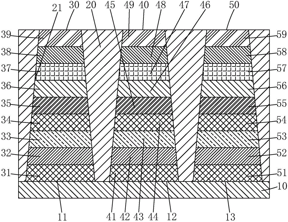
[0187] In the OLED display device of Example 1:
[0188] The red light OLED device comprises a first transparent conductive metal oxide layer 31, a first metal layer 32, a first PEDOT:PSS conductive film layer 33, a second transparent conductive Metal oxide layer 34, first hole injection layer 35, first hole transport layer 36, red light emitting layer 37, first electron transport layer 38, and first cathode 39;
[0189] The thickness of the first transparent conductive metal oxide layer 31 is 20nm; the thickness of the first metal layer 32 is 150nm; the thickness of the first PEDOT:PSS conductive film layer 33 is x R nm; the thickness of the second transparent conductive metal oxide layer 34 is 20nm; the material of the first hole injection layer 35 is HAT (CN) 6 , with a thickness of 5nm; the material of the first hole transport layer 36 is HTM081, with a thickness of 20nm; the red light-emitting layer 37 includes host material CBP and red phosphorescent dye Ir (DBQ) 2 (a...
PUM
 Abstract
Description
Claims
Application Information
 - R&D Engineer
- R&D Manager
- IP Professional
- Industry Leading Data Capabilities
- Powerful AI technology
- Patent DNA Extraction
Browse by: Latest US Patents, China's latest patents, Technical Efficacy Thesaurus, Application Domain, Technology Topic, Popular Technical Reports.
© 2024 PatSnap. All rights reserved.Legal|Privacy policy|Modern Slavery Act Transparency Statement|Sitemap|About US| Contact US: help@patsnap.com


