OLED display panel, manufacturing method, drive method and display device

A technology for display panels and manufacturing methods, which can be applied to static indicators, semiconductor/solid-state device manufacturing, instruments, etc., can solve the problems of overall structure thickness and poor flexibility and curvature, and achieve the goals of reducing thickness, improving brightness and flexibility and curvature Effect

Active Publication Date: 2017-03-15
BOE TECH GRP CO LTD
View PDF6 Cites 19 Cited by
  • Summary
  • Abstract
  • Description
  • Claims
  • Application Information

AI Technical Summary

Problems solved by technology

That is, in the AMOLED display panel of the prior art, the touch screen 15 is separately arranged above the light-emitting unit (including the driving backplane 11, the light-emitting layer 12, and the cathode layer 13), and then the touch screen 15 is arranged on the top of the touch screen 15. A circular polarizer that reduces external light reflection and enhances contrast, but the AMOLED display panel with this structure has the problems of thicker overall structure and poor flexibility and curvature

Method used


Image

  • OLED display panel, manufacturing method, drive method and display device
  • OLED display panel, manufacturing method, drive method and display device
  • OLED display panel, manufacturing method, drive method and display device

Examples


Embodiment Construction

[0045] The implementation process of the embodiment of the present invention will be described in detail below in conjunction with the accompanying drawings. It should be noted that the same or similar reference numerals represent the same or similar elements or elements having the same or similar functions throughout. The embodiments described below by referring to the figures are exemplary only for explaining the present invention and should not be construed as limiting the present invention.

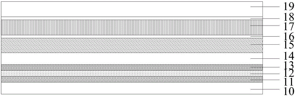
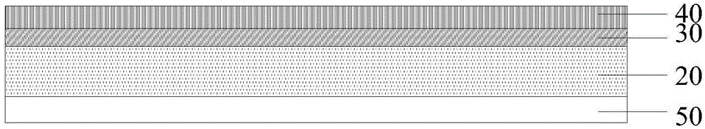
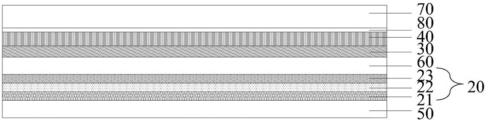
[0046] An embodiment of the present application provides an OLED display panel, see Figure 2-6As shown, the display panel includes: a light emitting unit 20 , and a quarter-wave plate 30 and a wire grid polarizer 40 sequentially disposed on the light emitting unit 20 . Wherein, the light-emitting unit 20 includes a driving backplane 21, a light-emitting layer 22, and a cathode layer 23. The cathode layer 23 includes a plurality of cathode sub-electrodes 231 extending along the first...


PUM


Abstract

The invention provides an OLED display panel, a manufacturing method, a drive method and a display device to reduce the thickness of the OLED display panel and to improve the brightness and the flexible bending degree of the OLED display panel. The OLED display panel comprises a light-emitting unit, a quarter-wave plate and a wire grid polarizer, wherein the quarter-wave plate and the wire grid polarizer are sequentially arranged on the light-emitting unit; the light-emitting unit comprises a drive backboard, a light-emitting layer and a cathode layer; the cathode layer comprises a plurality of cathode sub-electrodes which extend along a first direction and are insulated with one another; the cathode sub-electrodes transmit cathode signals during a display stage of the display panel and transmit touch drive signals during a touch stage of the display panel; the wire grid polarizer comprises a plurality of metal wires which extend along a second direction; at least one part of metal wires form a plurality of touch induction electrodes; the touch induction electrodes transmit touch induction signals during the touch stage of the display panel; and the second direction is intersected with the first direction.

Description

technical field [0001] The present application relates to the display field, in particular to an OLED display panel, a manufacturing method, a driving method and a display device. Background technique [0002] Current display types mainly include liquid crystal display (Liquid Crystal Display, LCD), organic light-emitting diode display (Organic Light-Emitting Diode, OLED), plasma display (Plasma Display Panel, PDP) and electronic ink display. Among them, the Active-matrix organic light emitting diode (AMOLED) in the OLED display is a new type of display device, which has high chromaticity, high contrast, wide viewing angle, high brightness, self-illumination, and fast response. , can realize flexible display and other characteristics, has been recognized as the next generation of flat panel display technology. [0003] like figure 1 Shown is a schematic structural diagram of an AMOLED display panel in the prior art, including a driving backplane 11, a light-emitting layer ...

Claims


Application Information

Patent Timeline
Patent Type & Authority Applications(China)
IPC IPC(8): H01L27/32H01L51/52H01L51/56G09G3/32
CPCG09G3/3208H10K59/40H10K59/121H10K50/86H10K59/1201H10K71/00G06F3/0412G06F3/044G09G3/3225G02B5/3083G06F2203/04112G02B5/3058H10K50/822G09G2320/0233G06F2203/04103H10K50/844H10K59/35H10K59/131
Inventor 王海生董学刘英明丁小梁吴俊纬许睿
Owner BOE TECH GRP CO LTD
Why Eureka
Try Eureka