Test structure and its formation method, test method

A test structure and test area technology, which is applied in the direction of measuring electricity, measuring devices, measuring electrical variables, etc., can solve the problems of poor heat dissipation capacity of fins and poor performance of fin field effect transistors, etc.

Active Publication Date: 2020-03-10
SEMICON MFG INT (SHANGHAI) CORP +1
View PDF1 Cites 0 Cited by
  • Summary
  • Abstract
  • Description
  • Claims
  • Application Information

AI Technical Summary

Problems solved by technology

[0004] However, as the size of semiconductor devices continues to shrink, the distance between the fins becomes smaller, resulting in poor heat dissipation between the fins, and the heat accumulation in the fins easily causes the performance of the FinFET to deteriorate.

Method used


Image

  • Test structure and its formation method, test method
  • Test structure and its formation method, test method
  • Test structure and its formation method, test method

Examples


Embodiment Construction

[0037] As mentioned in the background, as the size of semiconductor devices shrinks, the distance between the fins becomes smaller, which leads to heat accumulation in the fins, which causes the performance of the FinFET to deteriorate.

[0038] After research, it is found that when the transistor is working, due to the current generated in the channel region in the substrate, the channel region is equivalent to a resistance, that is, heat will be generated when the channel region is turned on; and the channel region Heating causes the substrate to heat up. For the FinFET, the channel region is formed in the fin, and when the channel region is turned on, the fin will generate heat.

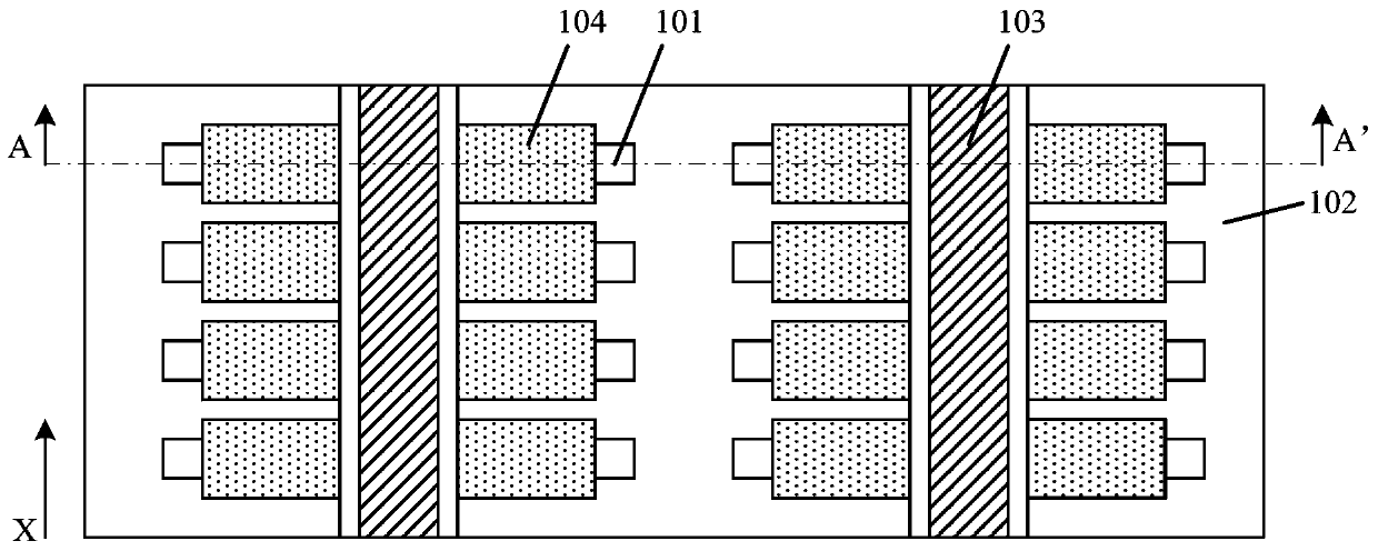
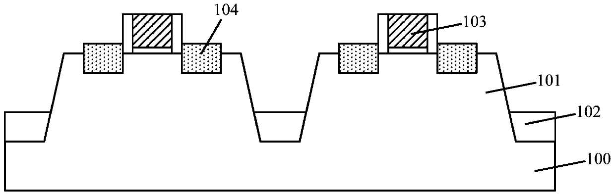
[0039] Please refer to figure 1 and figure 2 , figure 1 is a schematic top view structure diagram of a fin field effect transistor according to an embodiment of the present invention, figure 2 yes figure 1 A schematic cross-sectional structure along the direction AA', including: a substrate...


PUM


Abstract

The invention provides a testing structure and a forming method and a testing method thereof. The testing structure comprises a substrate, wherein the substrate comprises a heating region and a testing region adjacent to each other; a first grid structure disposed at the substrate surface of the heating region; a second grid structure disposed at the substrate surface of the testing region; a common source region disposed in the substrate between the first grid structure and the second grid structure; a first drain region disposed in the substrate in the heating region, wherein the first drain region and the common source region are disposed at the two sides of the first grid structure; a second drain region disposed in the substrate in the testing region, wherein the second drain region and the common source region are disposed at the two sides of the second grid structure. The testing structure can be used to test the influence of substrate self-heating upon the electric performance of a transistor.

Description

technical field [0001] The invention relates to the technical field of semiconductor manufacturing, in particular to a test structure, a forming method and a test method thereof. Background technique [0002] With the rapid development of semiconductor manufacturing technology, semiconductor devices are developing towards higher element density and higher integration. As the most basic semiconductor device, transistors are currently being widely used. Therefore, with the increase of component density and integration of semiconductor devices, the gate size of planar transistors is getting shorter and shorter. The ability of traditional planar transistors to control channel current Weakened, resulting in short channel effect, resulting in leakage current, and ultimately affecting the electrical performance of semiconductor devices. [0003] In order to overcome the short-channel effect of the transistor and suppress the leakage current, a Fin Field Effect Transistor (Fin FET)...

Claims


Application Information

Patent Timeline
Patent Type & Authority Patents(China)
IPC IPC(8): H01L21/334H01L21/77H01L29/06H01L27/02G01R31/27
CPCG01R31/275H01L21/77H01L27/088H01L29/0603H01L29/0684H01L29/66409
Inventor 周飞
Owner SEMICON MFG INT (SHANGHAI) CORP
Why Eureka
Try Eureka