Unit package body die and precise forming die for chip region exposed package

A chip area and package technology, applied in electrical components, semiconductor/solid-state device manufacturing, circuits, etc., can solve the problems of fit clearance, interference fit, affecting the function of the exposed area of ​​the chip, etc., so as to reduce the processing difficulty and ensure the processing accuracy. Effect

Pending Publication Date: 2017-02-22
SHANDONG SENSPIL ELECTRONICS TECH
View PDF5 Cites 2 Cited by
  • Summary
  • Abstract
  • Description
  • Claims
  • Application Information

AI Technical Summary

Problems solved by technology

Reason 2: There is a certain error in the chip loading process due to the different thickness of the glue on the chip, resulting in different heights of each chip after loading
Reason 3: There will be a certain machining error in the machining process of the boss on the top of the mold, which will cause the height of each boss to be different.
[0004] After the mold is closed, due to the above reasons, there will be a fit gap between the bosses of the mold and the chip, and some interference fits will appear.
If there is a gap between the two, there will be overflow on the top of the exposed area of ​​the chip during the packaging process, which will affect the function of the exposed area of ​​​​the chip, and the interference fit between the two will cause the chip to withstand the pressure of the boss on the top of the mold. risk of being crushed

Method used


Image

  • Unit package body die and precise forming die for chip region exposed package
  • Unit package body die and precise forming die for chip region exposed package
  • Unit package body die and precise forming die for chip region exposed package

Examples


Embodiment Construction

[0031] The present invention will be further described below in conjunction with the drawings and embodiments.

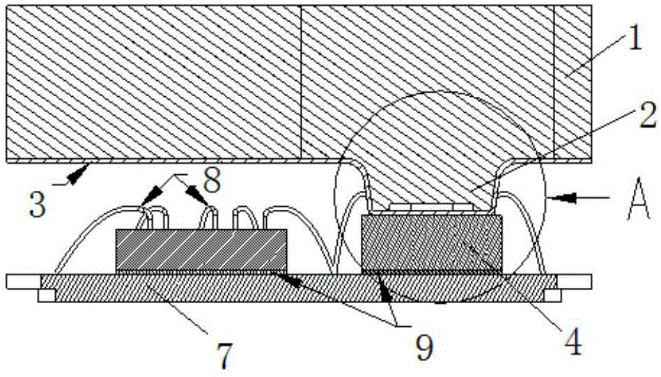
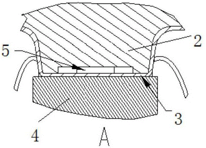
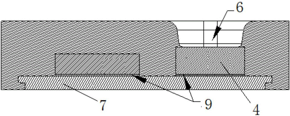
[0032] Such as Figure 5-Figure 6 As shown, a precision molding die for bare packaging of chip area includes multiple unit package molds 1 spliced ​​with each other, multiple unit package molds 1 are arranged in rows, and adjacent unit package molds 1 are spliced Combine into one. The multiple unit package molds 1 are arranged in rows and spliced ​​together to form a whole, which can be matched with multiple bare chips to realize packaging molding containing multiple bare chips.

[0033] Such as Figure 1-Figure 4 As shown, the unit package mold 1 includes a fixed support body 10, a movable molding assembly 11 is embedded at a set position in the fixed support body 10, a boss 2 is provided at one end of the molding assembly 11, and the other end of the molding assembly 11 and movable elements It cooperates to realize that the boss 2 protrudes and fixes the support body ...


PUM


Abstract

The invention discloses a unit package body die and precise forming die for chip region exposed package. The unit package body die comprises a fixed support body, wherein a movable forming assembly is embedded into a setting position of the fixed support body, a boss is arranged at one end part of the forming assembly and is used for pressing a chip, and the other end part of the forming assembly is in contact matching with a movable component so that the forming assembly moves in the fixed support body. In the forming die, a plurality of unit package body dies are arranged and are spliced with one another to form a whole, and package and forming of a plurality of exposed chips can be achieved; and each unit package body die is arranged in a split mode, the fixed support body is a support and positioning part for the whole unit package body die, the forming assembly is matched with the chip, the processing difficulty of the unit package body die can be reduced very well, and the processing accuracy is ensured.

Description

Technical field [0001] The invention belongs to the technical field of semiconductor chip packaging, and specifically relates to a unit package mold and a precision molding mold for bare packaging of a chip area. Background technique [0002] In order to achieve specific functions, some chips need to be partially exposed, and the exposed areas are specially treated, so that the treated exposed areas are in direct contact with the relevant media in the use environment, and various physical and chemical reactions occur to achieve specific effects Therefore, the exposed area does not need to be protected by plastic molding compound, while other areas still need to be protected by plastic molding compound. Compared with other areas, the exposed area after molding will appear in the form of grooves. The bottom of the groove is the exposed area of ​​the chip, and the side walls In order to protect the plastic compound in other areas, this form of packaging is called window packaging. I...

Claims


Application Information

Patent Timeline
Patent Type & Authority Applications(China)
IPC IPC(8): H01L21/67B29C44/34
CPCH01L21/67126B29C44/34
Inventor 邢广军刘昭麟崔广军栗振超
Owner SHANDONG SENSPIL ELECTRONICS TECH
Why Eureka
Try Eureka