Piezoelectric element, piezoelectric element application device, and method for manufacturing piezoelectric element
A piezoelectric element and a manufacturing method technology, which are applied in the manufacture/assembly of piezoelectric/electrostrictive devices, electrical components, piezoelectric/electrostrictive/magnetostrictive devices, etc., can solve the problem of reducing the characteristics of piezoelectric layers , The displacement of the piezoelectric element becomes smaller, and the displacement efficiency becomes lower.
- Summary
- Abstract
- Description
- Claims
- Application Information
AI Technical Summary
Problems solved by technology
Method used
Image
Examples
Embodiment approach 1
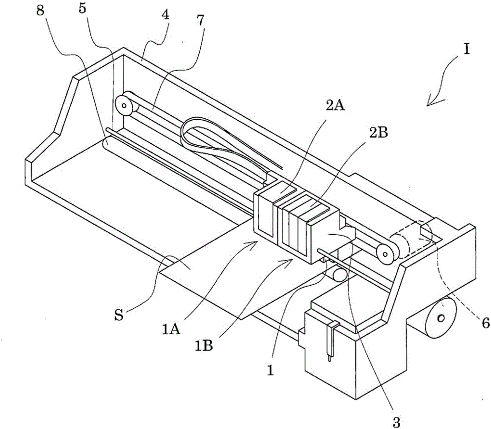
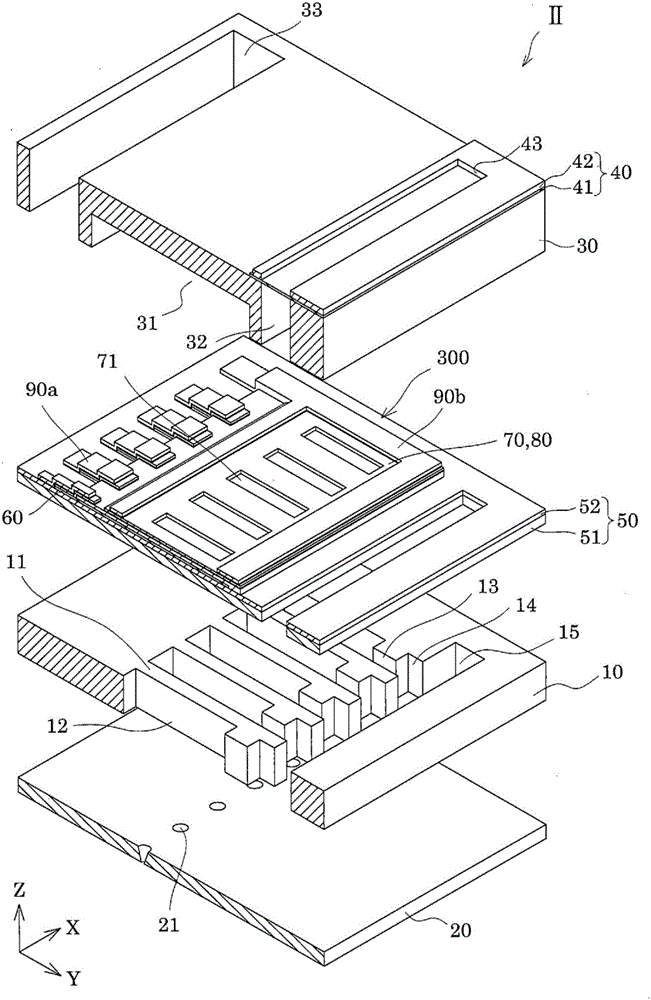
[0032] figure 1 It is an ink jet recording device as an example of a liquid ejecting device according to an embodiment of the present invention. As shown in the figure, in the ink jet recording apparatus I, in the ink jet recording head unit (head unit) II having a plurality of ink jet recording heads (refer to figure 2 ) is detachably provided with ink cartridges 2A and 2B constituting an ink supply unit. The carriage 3 to which the head unit II is attached is axially movable on a carriage shaft 5 attached to the apparatus main body 4 , and is a component that discharges black ink compositions and color ink compositions, respectively, for example.
[0033] Further, the driving force of the drive motor 6 is transmitted to the carriage 3 via a plurality of gears and the timing belt 7 not shown, so that the carriage 3 to which the head unit II is attached moves along the carriage shaft 5 . On the other hand, conveyance rollers 8 as conveyance means are provided on the apparat...
Embodiment
[0089] (Example)
[0090]
[0091] First, an elastic film 51 made of a silicon dioxide film with a thickness of 170 nm was formed on the surface by oxidizing the single crystal silicon substrate. Next, a zirconium film with a thickness of 285 nm was formed on the silicon dioxide film by a sputtering method, and the zirconium film was thermally oxidized to form an insulator film 52 made of a zirconium oxide film. Thereafter, a titanium film having a thickness of 20 nm was formed on the zirconium oxide film by sputtering, and the titanium film was thermally oxidized to form the adhesion layer 56 made of the titanium oxide film. Next, a first electrode 60 having a thickness of 130 nm was formed on the titanium oxide film by a sputtering method at 300° C. as a substrate with electrodes.
[0092]
[0093] The n-octane solution (both 0.5mol / L) of bismuth 2-ethylethanoate, iron 2-ethylethanoate, and titanium 2-ethylethanoate (both 0.5mol / L) was prepared according to the molar ra...
PUM
| Property | Measurement | Unit |
|---|---|---|
| coating thickness | aaaaa | aaaaa |
| coating thickness | aaaaa | aaaaa |
Abstract
Description
Claims
Application Information
 - R&D
- Intellectual Property
- Life Sciences
- Materials
- Tech Scout
- Unparalleled Data Quality
- Higher Quality Content
- 60% Fewer Hallucinations
Browse by: Latest US Patents, China's latest patents, Technical Efficacy Thesaurus, Application Domain, Technology Topic, Popular Technical Reports.
© 2025 PatSnap. All rights reserved.Legal|Privacy policy|Modern Slavery Act Transparency Statement|Sitemap|About US| Contact US: help@patsnap.com


