USB control circuit of a built-in signal junction circuit
A signal relay and control circuit technology, applied in electrical digital data processing, instruments, energy-saving computing, etc., can solve problems such as inability to switch, limitations, and the inability of USB host devices and USB peripheral devices to perform normal data transmission.
- Summary
- Abstract
- Description
- Claims
- Application Information
AI Technical Summary
Problems solved by technology
Method used
Image
Examples
Embodiment Construction
[0039] Embodiments of the present invention will be described below in conjunction with related drawings. In the drawings, the same reference numerals represent the same or similar elements or method flows.
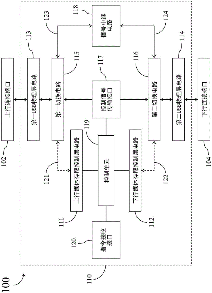
[0040] figure 1 It is a simplified functional block diagram of the USB hub device 100 according to an embodiment of the present invention. The USB hub device 100 includes an uplink port 102 , a downlink port 104 , and a USB control circuit (USB control circuit) 110 . exist figure 1 In the embodiment of the present invention, the USB control circuit 110 includes: an upstream media access control layer circuit (upstream MAC-layer circuit) 111, a downstream media access control layer circuit (downstream MAC-layer circuit) 112, a first USB physical layer circuit (USB PHY-layer circuit) 113, a second USB physical layer circuit 114, a first switching circuit (switch circuit) 115, a second switching circuit 116, a control signal transmission interface (control signal transmis...
PUM
 Abstract
Description
Claims
Application Information
 - R&D Engineer
- R&D Manager
- IP Professional
- Industry Leading Data Capabilities
- Powerful AI technology
- Patent DNA Extraction
Browse by: Latest US Patents, China's latest patents, Technical Efficacy Thesaurus, Application Domain, Technology Topic, Popular Technical Reports.
© 2024 PatSnap. All rights reserved.Legal|Privacy policy|Modern Slavery Act Transparency Statement|Sitemap|About US| Contact US: help@patsnap.com


