OLED (organic light emitting diode) display
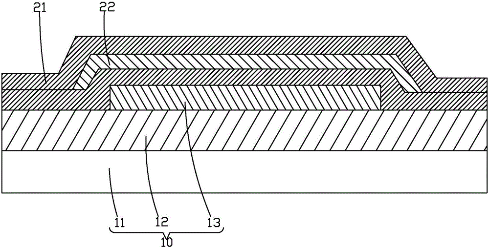
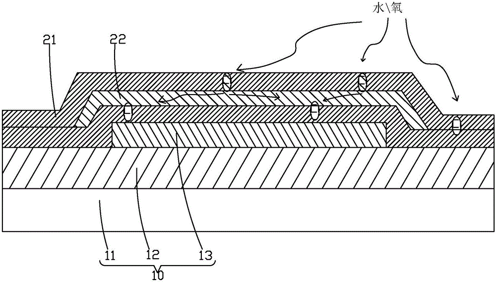
A display and display area technology, applied in the field of OLED displays, can solve problems such as increasing defects, micro-cracks, and inorganic film 22 defects, and achieve the effects of reducing the number and thickness of layers, improving service life, and improving bending performance
- Summary
- Abstract
- Description
- Claims
- Application Information
AI Technical Summary
Problems solved by technology
Method used
Image
Examples
Embodiment Construction
[0038] In order to further illustrate the technical means adopted by the present invention and its effects, the following describes in detail in conjunction with preferred embodiments of the present invention and accompanying drawings.
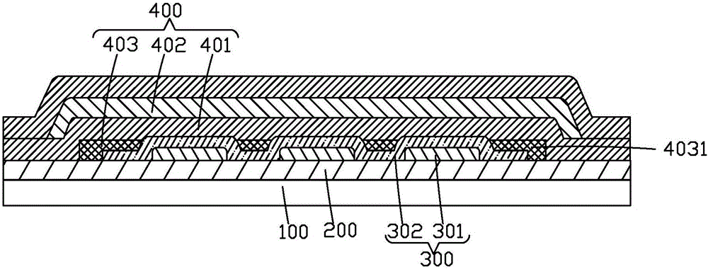
[0039] see image 3 , is a schematic structural view of the first embodiment of the OLED display of the present invention. In this embodiment, the OLED display includes a base substrate 100, a TFT array layer 200 disposed on the base substrate 100, and a The OLED layer 300 on the TFT array layer 200 , and the thin film encapsulation layer 400 disposed on the TFT array layer 200 and the OLED layer 300 and covering the OLED layer 300 .
[0040] The thin film encapsulation layer 400 includes an inorganic passivation layer 401, an organic buffer layer 402, and a water oxygen quenching layer 403; in the thin film encapsulation layer 400, the inorganic passivation layer 401 and the organic buffer layer 402 are alternately stacked, and the inorganic ...
PUM
 Abstract
Description
Claims
Application Information
 - R&D
- Intellectual Property
- Life Sciences
- Materials
- Tech Scout
- Unparalleled Data Quality
- Higher Quality Content
- 60% Fewer Hallucinations
Browse by: Latest US Patents, China's latest patents, Technical Efficacy Thesaurus, Application Domain, Technology Topic, Popular Technical Reports.
© 2025 PatSnap. All rights reserved.Legal|Privacy policy|Modern Slavery Act Transparency Statement|Sitemap|About US| Contact US: help@patsnap.com


