Micro cold and hot shock test device for electronic product
A technology of cold and thermal shock and test device, which is applied in measuring devices, instruments, scientific instruments, etc., can solve the problems of large environmental pollution, large space occupation, waste of energy, etc., achieve good thermal insulation effect, solve large space occupation, The effect of reducing the size of the device
- Summary
- Abstract
- Description
- Claims
- Application Information
AI Technical Summary
Problems solved by technology
Method used
Image

Examples
Embodiment 1
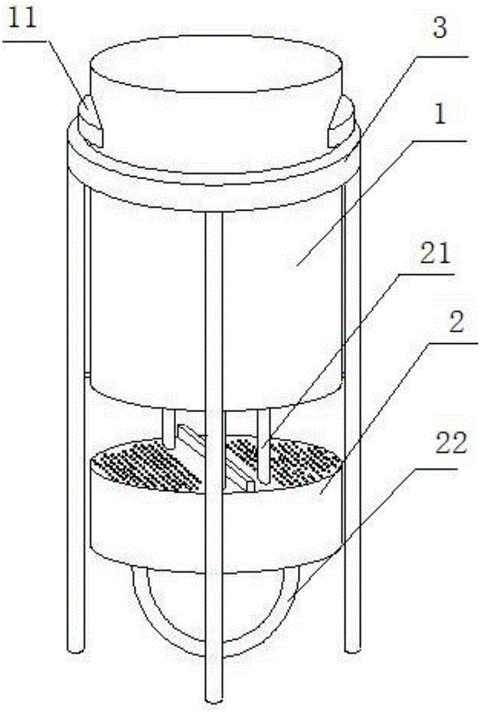
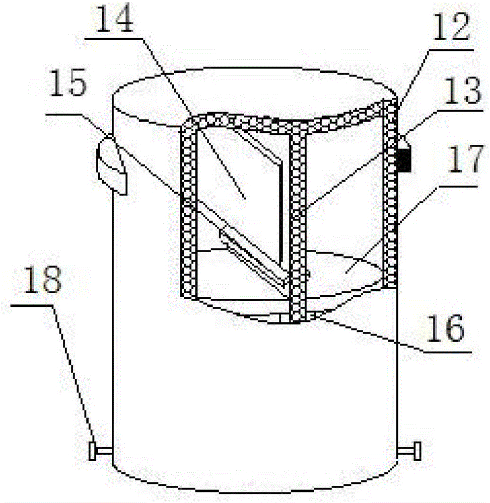
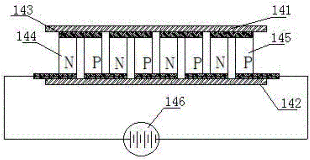
[0026] Such as Figure 1-Figure 3 As shown, a miniature cold and thermal shock test device for electronic products includes a test body 1 and a test sample mounting base 2 that are movable up and down. The thermal insulation shell 12 is cylindrical with an open lower end, and a thermal insulation partition 13 is arranged inside the thermal insulation casing 12. The thermal insulation partition 13 and the test sample installation base 2 separate the thermal insulation casing 12 into a cold test room and a hot test chamber independently arranged on the left and right sides. In the laboratory, the upper half of the insulation partition 13 is inlaid with a semiconductor refrigeration device 14, and the semiconductor refrigeration device 14 is composed of a cold end surface 141, a hot end surface 142, a metal conductor 143, an N-type semiconductor 144, a P-type semiconductor 145 and a DC power supply 146. Composition, the material of the cold end face 141 and the hot end face 142 i...
Embodiment 2
[0031] Such as Figure 4-Figure 5 As shown, further optimization is carried out on the basis of a miniature thermal shock test device for electronic products described in Example 1, the inner wall of the heat preservation shell 12 is provided with a limiting block 15 and a sealing ring plate 16, and the limiting The block 15 is located below the semiconductor refrigeration device 14; the heat preservation shell 12 is provided with a movable sealing plate 17, and the movable sealing plate 17 is arranged between the limiting block 15 and the sealing ring plate 16, and the movable sealing plate 17 is installed on the base of the test sample. 2, the contact surface between the movable sealing plate 17 and the sealing ring plate 16 is provided with a sealing ring 19.
[0032] In this embodiment, the arrangement of the movable sealing plate 17 and the sealing ring plate 16 is to reduce the heat exchange between the cold test room and the hot test room and the environment when changi...
Embodiment 3
[0034] Such as Figure 6 As shown, further optimization is carried out on the basis of a miniature thermal shock test device for electronic products described in Example 2. The test sample mounting base 2 includes a cylindrical shell with an open upper end, and the outer shell of the shell The diameter is equal to the inner diameter of the heat preservation shell 12, and the inner wall of the shell is provided with an insulating layer, and the shell is provided with two upper plates 23 and two lower plates 25 sequentially from top to bottom, and between the upper plate 23 and the lower plate 25 A base partition 26 is provided, and the cavity 24 between the upper plate 23 and the lower plate 25 is divided into left and right parts corresponding to the cold test room and the hot test room, and several threaded through holes are evenly distributed on the upper plate 23 231, the upper plate 23 is connected to the movable sealing plate 17 on the same side, a number of small holes a...
PUM
 Abstract
Description
Claims
Application Information
 - R&D
- Intellectual Property
- Life Sciences
- Materials
- Tech Scout
- Unparalleled Data Quality
- Higher Quality Content
- 60% Fewer Hallucinations
Browse by: Latest US Patents, China's latest patents, Technical Efficacy Thesaurus, Application Domain, Technology Topic, Popular Technical Reports.
© 2025 PatSnap. All rights reserved.Legal|Privacy policy|Modern Slavery Act Transparency Statement|Sitemap|About US| Contact US: help@patsnap.com