A kind of LED chip cleaning and drying device

A drying device and wafer cleaning technology, which is applied in the field of lighting, can solve problems such as wafer surface pollution, and achieve the effects of improving good rate, simple structure, and saving resources

Active Publication Date: 2018-11-16
六安联众工业自动化技术有限公司
View PDF4 Cites 0 Cited by
  • Summary
  • Abstract
  • Description
  • Claims
  • Application Information

AI Technical Summary

Problems solved by technology

[0004] The technical problem to be solved by the present invention is to provide a method that can solve the problem that the surface of the wafer is polluted during the production process of the LED wafer.

Method used


Image

  • A kind of LED chip cleaning and drying device
  • A kind of LED chip cleaning and drying device

Examples


Embodiment Construction

[0019] In order to enable those skilled in the art to better understand the technical solutions of the present invention, the present invention will be further described in detail below in conjunction with the accompanying drawings.

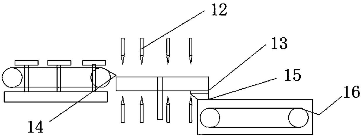
[0020] Please refer to figure 1 , figure 1 It is a structural schematic diagram of a specific embodiment provided by the present invention.

[0021] A cleaning and drying device for LED wafers, including an operating table, a turntable and a drying cylinder, a conveyor belt A is arranged above the operating table, and several rotatable brushes are provided on the operating table for brushing off particles on the surface of the wafer ; One end of the brush is located on the console, the other end is located above the conveyor belt A, close to the upper surface of the conveyor belt A; one side of the turntable is connected to the upper cover through a hinge; the center of the turntable is provided with a rotating shaft, the rotating shaft Several...


PUM


Abstract

The invention relates to an LED wafer cleaning and drying device. The LED wafer cleaning and drying device comprises an operating platform, a turnplate and a drying drum, wherein a conveyor belt A is arranged above the operating platform; a plurality of rotatable brushes for brushing particles on the surface of a wafer are arranged on the operating platform; one ends of the brushes are positioned on the operating platform; the other ends of the brushes are positioned above the conveyor belt A and are tightly adhered to the upper surface of the conveyor belt A; one side of the turnplate is connected with an upper cover through a hinge; a rotating shaft is arranged in the center of the inner part of the turnplate; the rotating shaft is connected with a plurality of rotating vanes; a plurality of liquid draining holes are formed in the bottom of the turnplate; the turnplate is connected with the drying drum through a transfer drum; a conveying plate B is arranged inside the drying drum; spray nozzles are formed above and below the turnplate. The LED wafer cleaning and drying device can solve the problem that in the LED wafer producing process, the surface of the wafer is contaminated.

Description

Technical field: [0001] The invention relates to an LED wafer cleaning and drying device, belonging to the lighting field. Background technique: [0002] The manufacturing process of LED chips: epitaxial wafer→cleaning→plating transparent electrode layer→transparent electrode pattern lithography→corrosion→remove glue→platform pattern lithography→dry etching→glue removal→annealing→SiO2 deposition→window pattern lithography →SiO2 corrosion→gel removal→N pole pattern photolithography→pre-cleaning→coating→stripping→annealing→P pole pattern photolithography→coating→stripping→grinding→cutting→chip→finished product testing. [0003] Cleaning is a particularly important link in the production process. If the cleaning is not thorough, the wafer will be unusable and cause great waste. Invention content: [0004] The technical problem to be solved by the present invention is to provide a method that can solve the problem that the surface of the wafer is polluted during the productio...

Claims


Application Information

Patent Timeline
Patent Type & Authority Patents(China)
IPC IPC(8): H01L33/00H01L21/67
CPCH01L21/67034H01L21/67046H01L21/67051H01L33/005
Inventor 赵少芹
Owner 六安联众工业自动化技术有限公司
Why Eureka
Try Eureka