
Manufacturing method of polycrystalline silicon and manufacturing method of monocrystalline silicon

A manufacturing method, single crystal silicon technology, applied in the direction of single crystal growth, polycrystalline material growth, chemical instruments and methods, etc., can solve the problems of high cost, high price, slow growth speed, etc., and achieve low manufacturing cost and high production efficiency High, fast-growing effect

Inactive Publication Date: 2017-01-04
丁欣
View PDF4 Cites 5 Cited by
  • Summary
  • Abstract
  • Description
  • Claims
  • Application Information

AI Technical Summary

Problems solved by technology

The disadvantage of the trichlorosilane Siemens method is that the reaction temperature is high, and expensive high-purity graphite needs to be used as the chuck of the silicon core. More importantly, high-purity graphite is a source of carbon pollution, and the finished product that is in contact with graphite Polysilicon is called carbon head material in the industry, and it can only be used as a waste product, causing huge waste; the growth rate is slow, and the current mainstream technology 130-150 mm diameter silicon rod takes about 60 hours or more to complete the growth; trichlorosilane The conversion is low due to the reaction of SiHCl 3 +HCl->SiCl 4 +H 2 A large number of by-products of silicon tetrachloride are produced, so it is necessary to separate silicon tetrachloride from the tail gas and convert it into trichlorosilane for recycling, while the annual production of 10,000 tons of polysilicon requires the separation of more than 100,000 tons of tetrachloride in the tail gas The construction cost and energy consumption of silicon carbide, tail gas separation and silicon tetrachloride devices are astonishing; the production pressure of the pressurized reduction reactor is about 5 atmospheres, and it must be constructed in accordance with the Chinese national standard or the pressure vessel safety supervision standards of the country where the American ASME pressure vessel is located. , the cost is extremely high; the current mainstream technology increases the logarithm of silicon rods in the Siemens reactor to relatively reduce the energy lost on the surface of the reactor to reduce energy consumption. For example, the current industrialized large-scale Siemens reduction furnace silicon rods The number of pairs is 36 pairs, 48 ​​pairs or even more, and designing and processing a Siemens reduction furnace with more pairs of silicon rods is a huge challenge, and the opportunity cost of trial and error is high
However, the granular silicon metal or carbon content of the current common fluidized bed production is relatively high, and the product quality is low
At the same time, the investment in the silane fluidized bed reactor is relatively high, which makes the production depreciation very high
This method requires the construction of a large-scale silane synthesis plant, and the explosive properties of silane are similar to hydrogen, which is prone to safety hazards
[0006] In addition, traditional monocrystalline silicon manufacturing usually adopts Czochralski or zone melting process, which needs to manufacture polysilicon first, and then pull and grow polysilicon. The consumables, energy consumption and equipment investment of single crystal pulling process are relatively large.
Moreover, when the traditional Czochralski method is used to manufacture single crystals, oxygen atoms and other impurities in the quartz crucible will enter the molten silicon and eventually affect the quality of single crystals
The so-called oxygen-free single crystal can be produced by the zone melting method, and the power consumption is lower than that of the Czochralski method; however, the crystal pulling equipment is much more complicated and expensive than that of the Czochralski method, and the production of the raw material polysilicon rods used in the production of the zone melting single crystal is also relatively difficult. Small output and high price, resulting in the market share of zone melting monocrystalline silicon being far smaller than that of Czochralski monocrystalline silicon

Method used


Image

  • Manufacturing method of polycrystalline silicon and manufacturing method of monocrystalline silicon
  • Manufacturing method of polycrystalline silicon and manufacturing method of monocrystalline silicon
  • Manufacturing method of polycrystalline silicon and manufacturing method of monocrystalline silicon

Examples


Embodiment Construction

[0024] In order to make the object, technical solution and advantages of the present invention clearer, the present invention will be described in detail below with reference to the accompanying drawings and embodiments.

[0025] In the present invention, the polycrystalline silicon is produced by the plasma enhanced chemical vapor deposition method, and the single crystal silicon is produced by the plasma enhanced chemical vapor deposition epitaxy method.

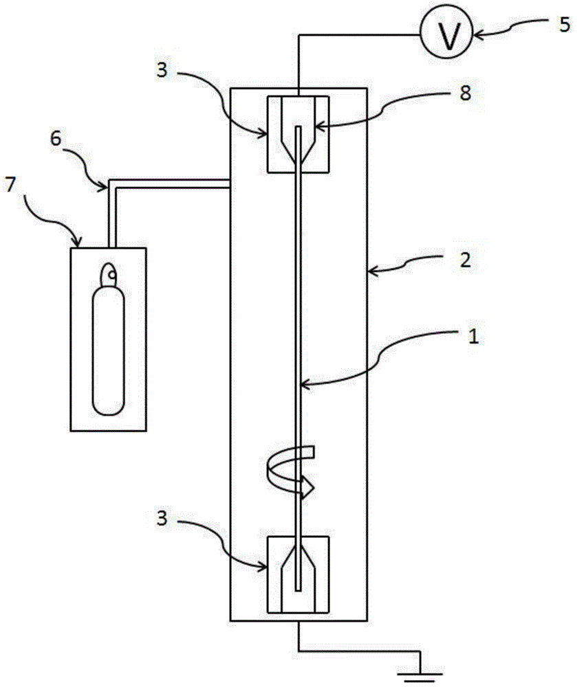
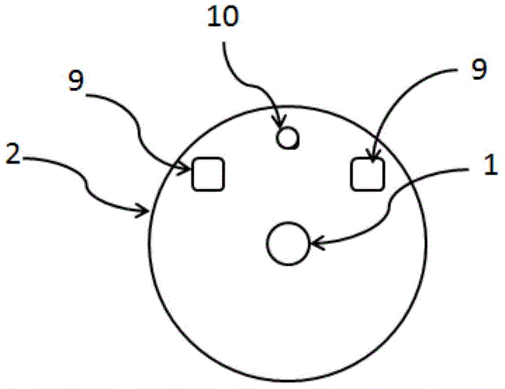
[0026] figure 1 It is a schematic diagram of the manufacturing apparatus used for the manufacturing method of polycrystalline silicon and single crystal silicon concerning this invention. like figure 1 As shown, the manufacturing device includes a reaction chamber 2 , a gas supply device 7 , a pipeline 6 and a power source 5 . The reaction chamber 2 can carry out the process reaction under normal pressure or a pressure lower than one atmospheric pressure, and it can be a cylinder, a cube or any shape convenient for arran...


PUM

PropertyMeasurementUnit
lengthaaaaaaaaaa

Abstract

The invention provides a manufacturing method of polycrystalline silicon. The method comprises the following steps of installing a silicon core into a reaction chamber; introducing reaction gas into the reaction chamber, wherein the reaction gas comprises silicon precursors, and the reaction gas further comprises hydrogen gas when the silicon precursors are chlorinated silane; exciting plasma from the reaction chamber or injecting plasma into the reaction chamber from an external plasma source; performing plasma enhancing chemical gas phase polycrystalline silicon deposition on the surface of one or a plurality of silicon chips by the reaction gas, wherein when the plurality of silicon chips are used, the silicon chips are mutually independent in the reaction chamber. The invention also provides a manufacturing method of monocrystalline silicon.

Description

technical field [0001] The present invention relates to a method for producing polycrystalline silicon and a method for producing monocrystalline silicon. Background technique [0002] The electronics and solar industries widely use high-purity silicon materials to manufacture integrated circuits, various discrete components, and solar cells. Before making these devices, high-purity polysilicon material needs to be obtained. Known methods for producing polycrystalline silicon include, for example, the trichlorosilane Siemens method, the silane Siemens method, and the silane fluidized bed method. [0003] Trichlorosilane Siemens method is currently the mainstream technology for manufacturing polysilicon. In this technique, thin silicon cores are bridged in pairs two by two, and the cores are heated by passing an electric current. Under the reaction conditions of 1 to 5 atmospheres and 1050-1100 degrees Celsius, trichlorosilane and hydrogen react SiHCl 3 +H 2 ->Si+3HCl...

Claims


Application Information

Patent Timeline
Patent Type & Authority Applications(China)
IPC IPC(8): C30B25/02C30B28/14C30B29/06
Inventor 丁欣
Owner 丁欣
Learn More