Array substrate and liquid display panel

An array substrate and substrate technology, applied in the field of liquid crystal display, can solve problems such as drift, unevenness, poor quality and effect of liquid crystal display, etc., and achieve the effect of reducing the drift of threshold voltage and uniform display effect

Active Publication Date: 2016-12-21
WUHAN CHINA STAR OPTOELECTRONICS TECH CO LTD
View PDF4 Cites 3 Cited by
  • Summary
  • Abstract
  • Description
  • Claims
  • Application Information

AI Technical Summary

Problems solved by technology

[0003] However, the current situation is that the threshold voltage of the oxide semiconductor TFT on the panel drifts, and the threshold voltage of each oxide semiconductor TFT varies greatly and is not uniform, which has a very bad influence on the quality and effect of the liquid crystal display.

Method used


Image

  • Array substrate and liquid display panel
  • Array substrate and liquid display panel
  • Array substrate and liquid display panel

Examples


Embodiment Construction

[0058] The present invention will be described in detail below in conjunction with the accompanying drawings and embodiments.

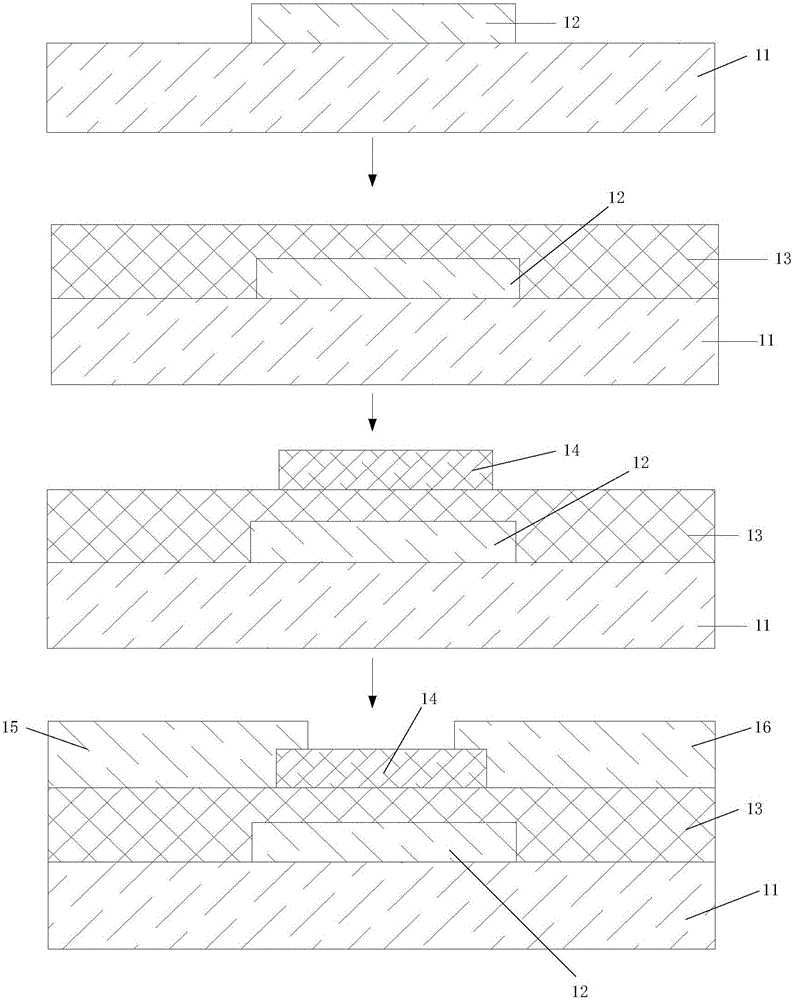
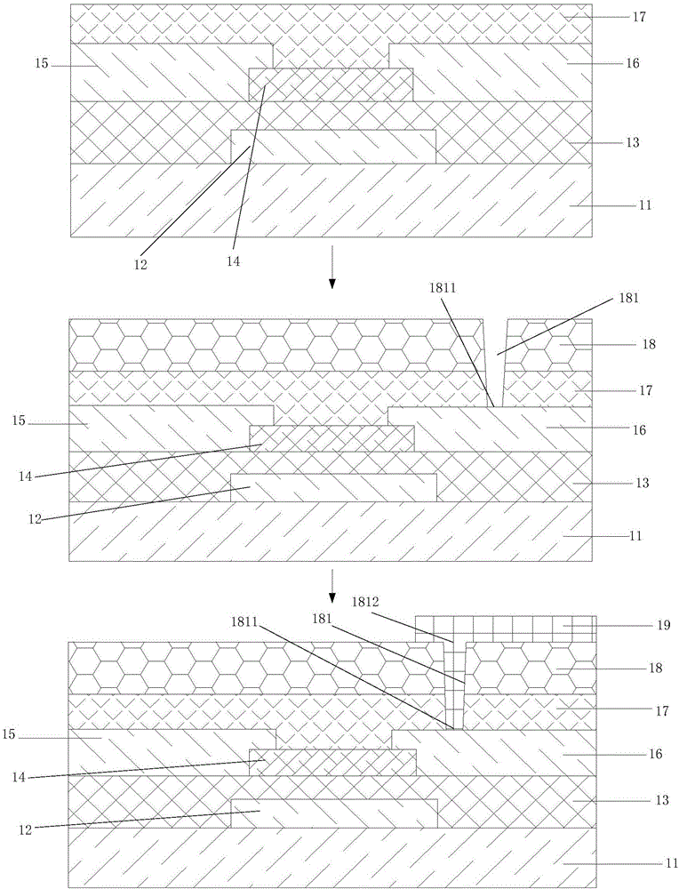
[0059] refer to figure 1 , figure 1 It is a schematic structural view of an embodiment of an array substrate of the present invention, wherein a plurality of oxide thin film transistors distributed in an array are arranged on the array substrate, and the array substrate includes: a substrate 11, a gate layer 12, a gate insulating layer 13, an oxide material semiconductor layer 14 , source layer 15 and drain layer 16 , passivation layer 17 , planar layer 18 and pixel electrode layer 19 .

[0060] The gate layer 12 is formed on the substrate 11 . The material of the gate layer 12 is a metal conductor material.

[0061] The gate insulating layer 13 covers the substrate 11 and the gate layer 12 . The material of the gate insulating layer 13 can be SiOx thin film, and the thickness can be less than 500nm.

[0062] The oxide semiconductor material laye...


PUM


Abstract

The invention discloses an array substrate and a liquid display panel. After an oxide semiconductor material layer is formed, annealing is carried out under the radio frequency irradiation in compressed air, so a passivation layer or a grid insulation layer is formed. In this way, multiple differences among threshold voltage of oxide thin film transistors can be adjusted, and drifting of the threshold voltage of the oxide thin film transistors TFT can be reduced, so a technical basis is provided for uniform display effects.

Description

technical field [0001] The invention relates to the technical field of liquid crystal display, in particular to an array substrate and a liquid crystal display panel. Background technique [0002] Oxide semiconductor TFT (Oxide semiconductor TFT) has the advantages of high mobility and relatively cheap large-area production, and is gradually becoming a strong competitor in the next generation of display technology. [0003] However, the current situation is that the threshold voltage of the oxide semiconductor TFT on the panel drifts, and the threshold voltage of each oxide semiconductor TFT varies greatly and is not uniform, which has a very bad influence on the quality and effect of the liquid crystal display. . Contents of the invention [0004] The technical problem mainly solved by the present invention is to provide an array substrate and a liquid crystal display panel, which can adjust the difference between the threshold voltages of multiple oxide thin film transi...

Claims


Application Information

Patent Timeline
Patent Type & Authority Applications(China)
IPC IPC(8): H01L27/12
CPCH01L27/1214G02F1/133345H01L21/02337H01L21/02164H01L21/02274H01L21/441H01L27/1225H01L27/1248H01L29/45H01L29/66969H01L29/78693G02F1/136227G02F1/1368G02F2202/10H01L21/02345H01L21/02565H01L21/02592H01L21/02631H01L21/0274H01L21/47635H01L27/1262H01L29/42356
Inventor 谢应涛
Owner WUHAN CHINA STAR OPTOELECTRONICS TECH CO LTD
Why Eureka
Try Eureka