A method for measuring the depth of decarburization layer of steel
A measurement method and technology of decarburization layer, which are applied to measurement devices, instruments, and the use of wave/particle radiation, etc. Simple operation and good statistical effect
- Summary
- Abstract
- Description
- Claims
- Application Information
AI Technical Summary
Problems solved by technology
Method used
Image
Examples
Embodiment 1
[0022] 75Cr1 high-carbon steel plate sample is used, and the sample structure is pearlite + a small amount of ferrite. The specific steps and parameters are as follows:
[0023] 1. Sample preparation: first cut out a 75Cr1 block sample, the sample size is: 25mm (board width direction) × 20mm (plate length direction) × 8mm (plate thickness direction), then clean the sample and make a 25× The 8mm cross-section is ground and polished, and then placed in the electronic probe sample chamber for observation and testing.
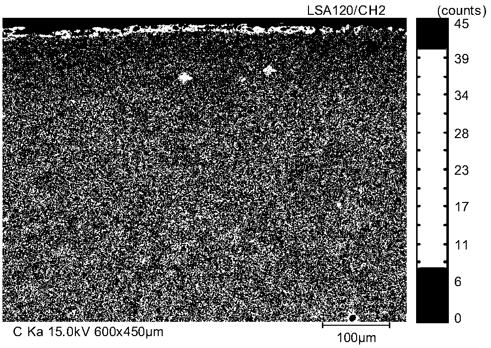
[0024] 2. Surface analysis: Open the "Mapping" module of the electronic probe analysis software, select C element as the analysis element, set the acceleration voltage to 15KV, the beam current to 50nA, the beam spot size to 1μm, the acquisition time to 5ms / point, and select the surface analysis area to be 600× 450μm, click "Operate" to conduct surface scanning analysis of C element, and obtain the surface distribution map of C element.
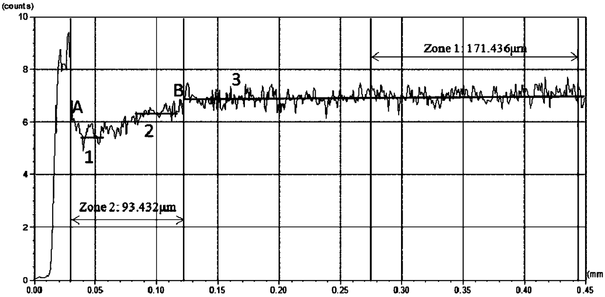
[0025] 3. Line analysis p...
Embodiment 2
[0033] Select a 20CrMnTi low carbon steel bar sample, the sample structure is martensite + a small amount of ferrite, the specific steps and parameters are as follows:
[0034] 1. Sample preparation: first cut 20CrMnTi sample, sample size: diameter The height is 20mm, and then the sample is cleaned and the cross-section is ground and polished, and then placed in the electronic probe sample chamber for observation and testing.
[0035] 2. Surface analysis: Open the "Mapping" module of the electronic probe analysis software, select C element as the analysis element, set the acceleration voltage to 15KV, the beam current to 50nA, the beam spot size to 1μm, the acquisition time to 15ms / point, and select the surface analysis area to be 2.5× 1.8mm, click "Operate" to conduct surface scanning analysis of C elements, and obtain the surface distribution map of C elements.
[0036]3. Line analysis processing: Carry out line analysis processing on the surface distribution map of C elem...
PUM
| Property | Measurement | Unit |
|---|---|---|
| diameter | aaaaa | aaaaa |
| length | aaaaa | aaaaa |
| width | aaaaa | aaaaa |
Abstract
Description
Claims
Application Information
 - R&D
- Intellectual Property
- Life Sciences
- Materials
- Tech Scout
- Unparalleled Data Quality
- Higher Quality Content
- 60% Fewer Hallucinations
Browse by: Latest US Patents, China's latest patents, Technical Efficacy Thesaurus, Application Domain, Technology Topic, Popular Technical Reports.
© 2025 PatSnap. All rights reserved.Legal|Privacy policy|Modern Slavery Act Transparency Statement|Sitemap|About US| Contact US: help@patsnap.com


