A laser annealing device and annealing method with energy compensation

A technology of laser annealing and energy compensation, used in laser welding equipment, manufacturing tools, welding equipment, etc., can solve the problems of affecting the overlay accuracy, large thermal deformation of silicon wafers, and long dwell time, avoiding pattern effects, dwell time and other problems. The effect of short residence time and reducing the effect of overlay accuracy

Active Publication Date: 2019-09-17
SHANGHAI MICRO ELECTRONICS EQUIP (GRP) CO LTD
View PDF7 Cites 0 Cited by
  • Summary
  • Abstract
  • Description
  • Claims
  • Application Information

AI Technical Summary

Problems solved by technology

Currently Ultratech uses CO with a wavelength of 10.6 μm 2 The P-polarized Brewster angle incident wafer of the laser has an annealing time of several hundred microseconds, which belongs to the sub-millisecond level. Currently, it is mainly used in the 28-45nm node. It is sub-millisecond annealing, which can basically meet the diffusion requirements at nodes above 28nm; but at nodes below 28nm, the diffusion requirements are around 2nm, and millisecond annealing is already difficult to meet this requirement
In addition, due to the long annealing time of the millisecond annealing, the dwell time of the annealing temperature is on the sub-millisecond scale, and the long dwell time is easy to cause thermal diffusion, resulting in large thermal deformation of the silicon wafer as a whole
In addition, it is necessary to preheat the workpiece table to improve heat absorption, and its overall thermal budget is relatively large, which will bring about thermal strain, easily cause stress deformation, and affect subsequent overlay accuracy

Method used


Image

  • A laser annealing device and annealing method with energy compensation
  • A laser annealing device and annealing method with energy compensation
  • A laser annealing device and annealing method with energy compensation

Examples


Embodiment Construction

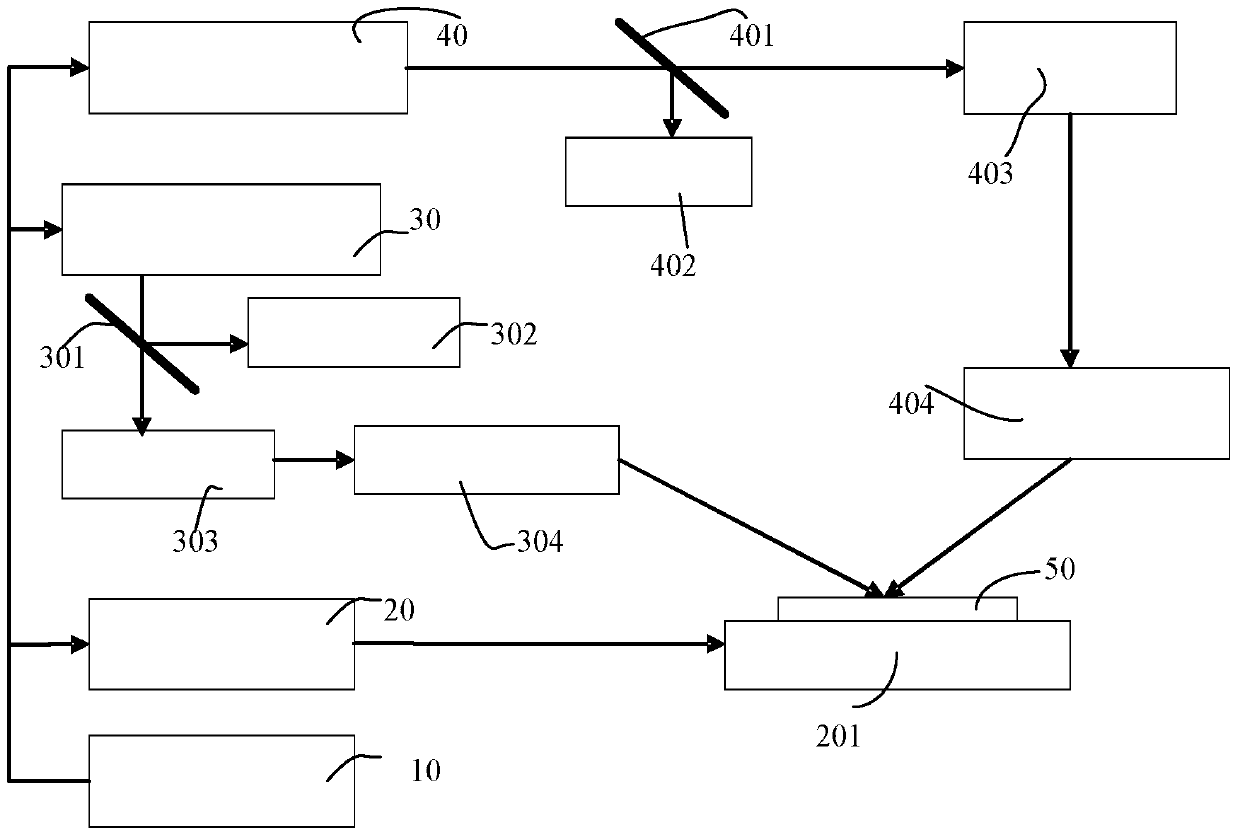
[0037] In order to make the above objects, features and advantages of the present invention more comprehensible, specific implementations of the present invention will be described in detail below in conjunction with the accompanying drawings. It should be noted that all the drawings of the present invention are in simplified form and use inaccurate scales, and are only used to facilitate and clearly assist the purpose of illustrating the embodiments of the present invention.

[0038] Please refer to figure 1 , a laser annealing device with energy compensation, comprising a loading table 201 for carrying a silicon wafer 50, driving the silicon wafer 50 for scanning annealing, and also including

[0039] The infrared laser 303 is used to emit infrared laser. The infrared laser uses Brewster's angle to preheat the silicon wafer 50. The infrared laser can be a pulsed laser or a continuous laser.

[0040] An infrared optical system 304, configured to perform optical system shapin...


PUM


Abstract

The invention discloses a laser annealing device with energy compensation. The laser annealing device comprises a control system, a chip holder, an infrared laser device and a pulse laser device. The infrared laser device emits infrared laser and preheats a silicon chip by the Brewster angle. The pulse laser device emits pulse laser and performs annealing on the silicon chip by the Brewster angle. The energy of infrared laser and pulse laser can be adjusted and superposed. The invention also discloses a laser annealing method. According to the laser annealing device with energy compensation, annealing is performed on the silicon chip by the Brewster angle so that temperature residing time is at the microsecond level, residing time is short and ion thermal diffusion can be reduced; and the workpiece holder does not need to be preheated so that thermal budge is low, thermal strain can be avoided, thermal stress deformation can be reduced and the influence on the overlay accuracy can be reduced. The energy of infrared laser and pulse laser can be adjusted and superposed so that the problem of the pattern effect can be avoided, the mechanical structure can be simplified and the cost can be saved.

Description

technical field [0001] The invention relates to a laser annealing device and an annealing method with energy compensation. Background technique [0002] In the past few decades, the manufacturing of electronic devices has followed Moore's Law and experienced rapid development. Reducing the size of integrated circuits is the driving force for maintaining this trend. However, with the reduction of manufacturing size, it has brought difficulties and challenges in manufacturing process technology . In the formation process of CMOS transistors, heat treatment has always played a key role, especially for key processes such as ultra-shallow junction activation and silicide formation. Traditional rapid annealing has been difficult to meet the requirements of 45nm and higher nodes. New annealing technologies to replace rapid thermal annealing are being studied extensively, such as flash lamp annealing, laser spike annealing, and low-temperature solid-phase epitaxy. Among them, lase...

Claims


Application Information

Patent Timeline
Patent Type & Authority Patents(China)
IPC IPC(8): H01L21/268B23K26/067
Inventor 兰艳平宋春峰
Owner SHANGHAI MICRO ELECTRONICS EQUIP (GRP) CO LTD
Why Eureka
Try Eureka