Display panel, manufacturing method thereof, and display device
A technology for display panels and array substrates, which is used in the manufacture of semiconductor/solid-state devices, semiconductor devices, electrical components, etc., can solve problems such as the display panel cannot be displayed normally, and achieve the effect of preventing normal display.
- Summary
- Abstract
- Description
- Claims
- Application Information
AI Technical Summary
Problems solved by technology
Method used
Image

Examples
Embodiment Construction
[0040] In order to make the object, technical solution and advantages of the present invention clearer, the implementation manner of the present invention will be further described in detail below in conjunction with the accompanying drawings.
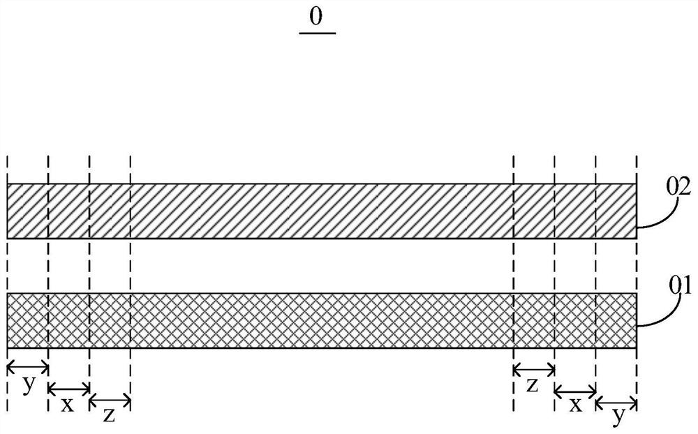
[0041] like figure 1 As shown, the embodiment of the present invention provides a display panel 0 , which may include: an array substrate 01 , and a package substrate 02 bonded to the array substrate 01 .
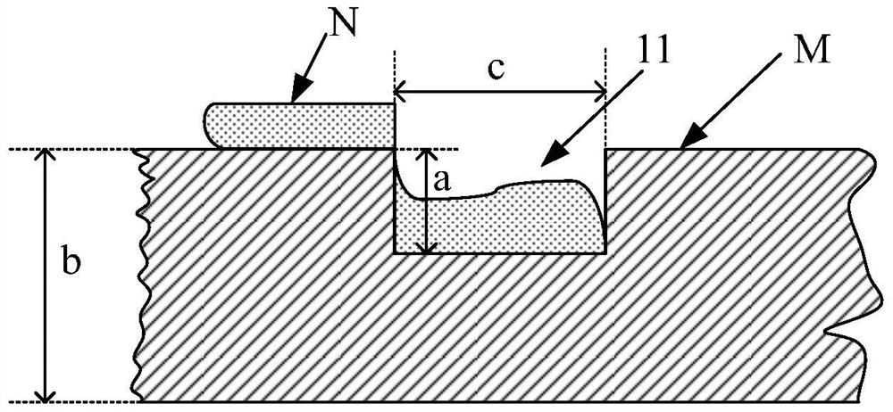
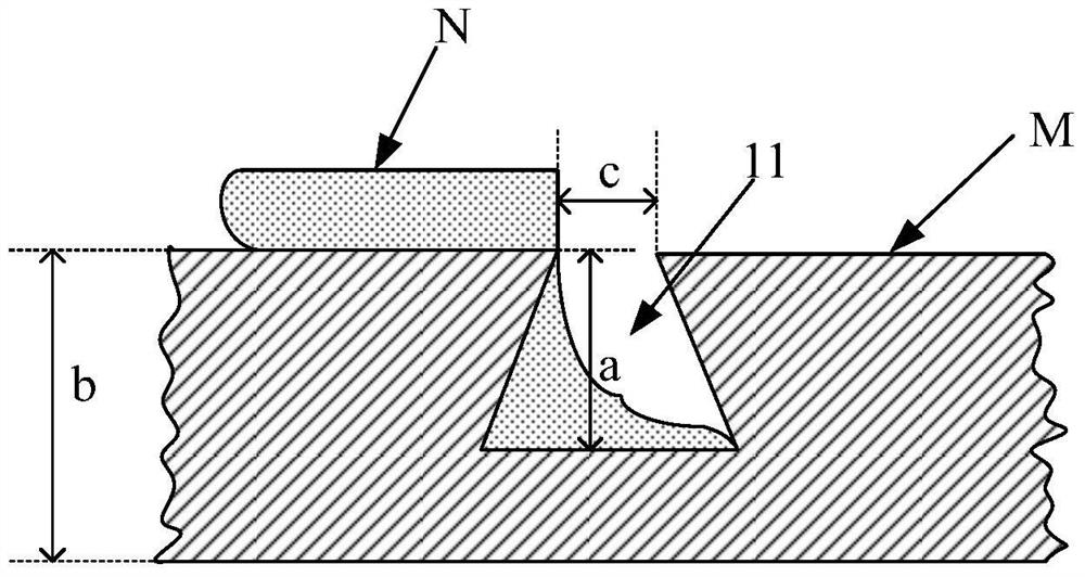
[0042] Wherein, a barrier portion ( figure 1 not shown in ), and the target area x includes: the area between the glass glue coating area y and the control circuit setting area z on the display panel 0 .
[0043] To sum up, the embodiment of the present invention provides a display panel, since a blocking portion is formed in the target area between the packaging substrate and the array substrate in the display panel, and the target area includes: glass glue coating on the display panel The area between the area and the control ci...
PUM
 Abstract
Description
Claims
Application Information
 - R&D
- Intellectual Property
- Life Sciences
- Materials
- Tech Scout
- Unparalleled Data Quality
- Higher Quality Content
- 60% Fewer Hallucinations
Browse by: Latest US Patents, China's latest patents, Technical Efficacy Thesaurus, Application Domain, Technology Topic, Popular Technical Reports.
© 2025 PatSnap. All rights reserved.Legal|Privacy policy|Modern Slavery Act Transparency Statement|Sitemap|About US| Contact US: help@patsnap.com