Printed circuit board and wireless communication device with printed circuit board
A technology for wireless communication devices and printed circuit boards, which is applied in the directions of printed circuits, printed circuit components, antenna supports/installation devices, etc., can solve the problems such as the influence of the volume of audio components, and achieves improved utilization and reduced parasitic capacitance. , Solve the effect of antenna interference
- Summary
- Abstract
- Description
- Claims
- Application Information
AI Technical Summary
Problems solved by technology
Method used
Image
Examples
Embodiment 1
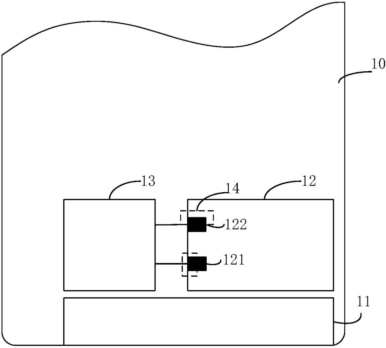
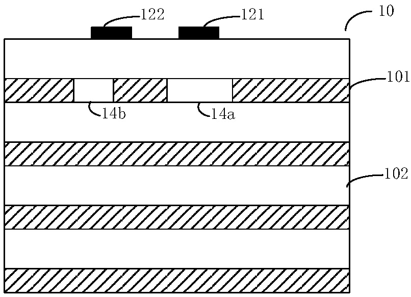
[0034] First, please refer to Figure 2 to Figure 4 The wireless communication device of this embodiment includes a printed circuit board 10, an antenna 11, an audio component 12, an audio circuit 13 and a parasitic capacitance reducing structure 14, and other components are not shown for convenience of description. Wherein, the printed circuit board 10 has a plurality of conductive layers 101 and a plurality of insulating layers 102 stacked vertically, and each insulating layer 102 is respectively disposed between each conductive layer 101 to isolate the lines of each conductive layer 101 . The audio component 12 is disposed on the top conductive layer, adjacent to the antenna, and has two electrical pins 121 , 122 directly connected to the audio circuit 13 . The electrical pins 121 and 122 are located on the top conductive layer, respectively forming two parallel plate capacitors with the next top conductive layer. The parasitic capacitance reducing structure 14 includes at...
Embodiment 2
[0036]The wireless communication device of this embodiment includes a printed circuit board 10 , an antenna 11 , an audio component 12 , an audio circuit 13 and a parasitic capacitance reducing structure 14 . Wherein, the printed circuit board 10 has a plurality of conductive layers 101 and a plurality of insulating layers 102 stacked vertically. The audio component 12 is located on the top conductive layer and adjacent to the antenna, and has two electrical pins 121 , 122 directly connected to the audio circuit 13 . The electrical pins 121, 122 are located on the top conductive layer. The parasitic capacitance reducing structure 14 includes two clear areas 14a and 14b disposed on the second top conductive layer and located below the electrical pins 121 and 122, and the two electrical pins 121 and 122 are completely located in the two clear areas respectively. Inside. The advantage of this is that the parallel plate capacitor is no longer formed between the electrical pin an...
PUM
 Abstract
Description
Claims
Application Information
 - Generate Ideas
- Intellectual Property
- Life Sciences
- Materials
- Tech Scout
- Unparalleled Data Quality
- Higher Quality Content
- 60% Fewer Hallucinations
Browse by: Latest US Patents, China's latest patents, Technical Efficacy Thesaurus, Application Domain, Technology Topic, Popular Technical Reports.
© 2025 PatSnap. All rights reserved.Legal|Privacy policy|Modern Slavery Act Transparency Statement|Sitemap|About US| Contact US: help@patsnap.com


