


Quick Research
Generate reliable direction feasibility study reports for your R&D in just a few steps.

Technical Q&A
Discover and master advanced knowledge NOW. Basics, ideas, possibilities, all at once.

Find Solutions
As an expert in R&D theories, this can generate solutions to your technical problems instantly.

Evaluate Feasibility
Analyze your overall solution with one click, know your potential R&D risks in advance.

Monitor Landscape
Get weekly tech updates, stay abreast of the latest tech innovations and key insights.
Semiconductor device, method of manufacturing semiconductor device, photodiode array, and imaging apparatus
A photodiode and semiconductor technology, applied in semiconductor/solid-state device manufacturing, semiconductor devices, diodes, etc., can solve problems such as quantum efficiency degradation, increase in the amount of light, degradation, etc., achieve good initial characteristics, reduce the number of layers, and reduce stress. Effect
- Summary
- Abstract
- Description
- Claims
- Application Information
AI Technical Summary
Problems solved by technology
Method used
Image

Examples
Embodiment 1
[0054]
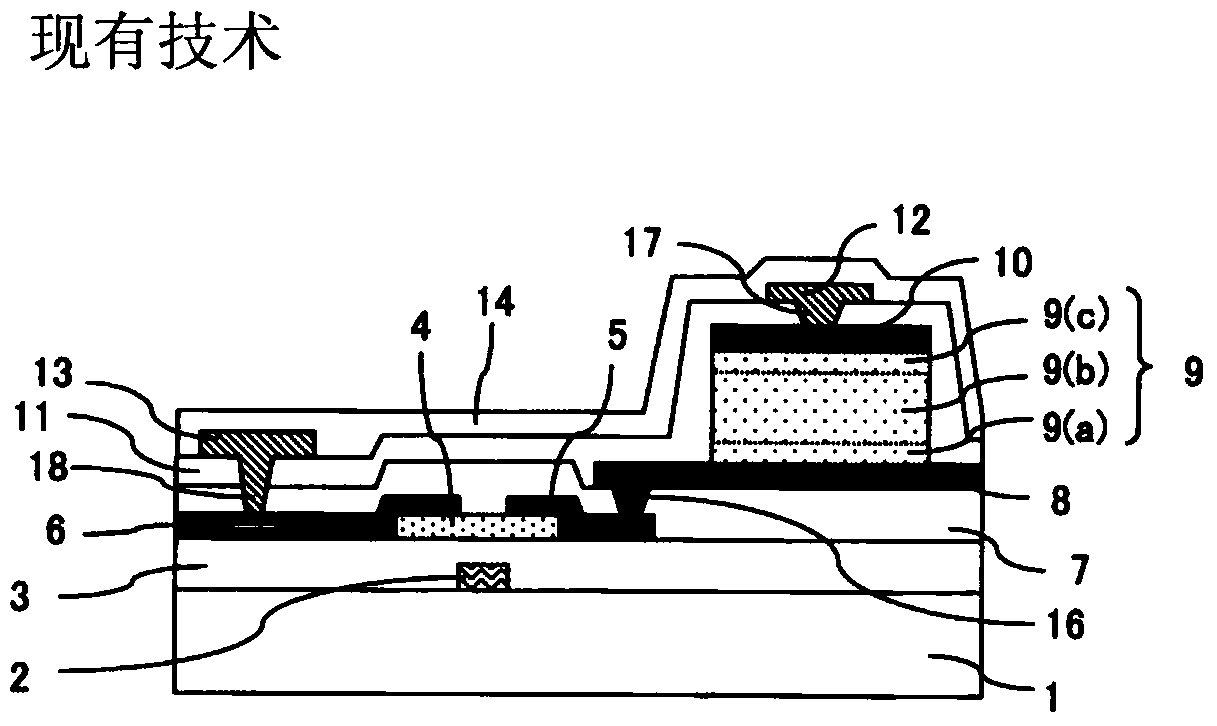
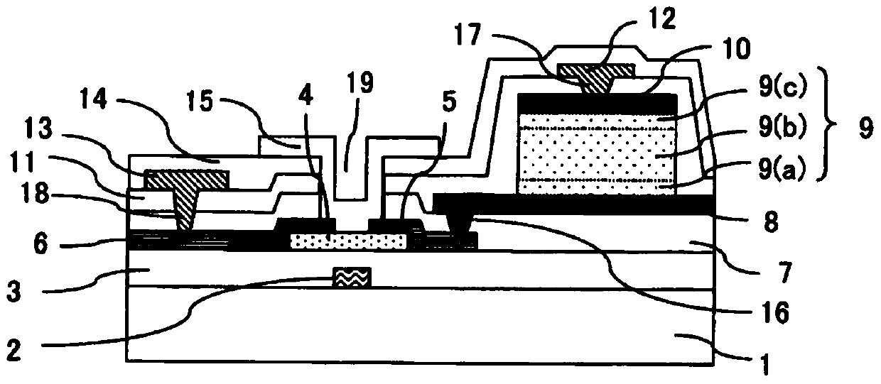
[0055] image 3 is a cross-sectional view of the element structure of the semiconductor device according to Embodiment 1 of the present invention. Figure 4 is a plan view schematically illustrating a circuit of a photodiode array. will describe image 3 The component structure shown in. In the upper layer of the oxide semiconductor layer 4, the source electrode 5 and the drain electrode 6 of the TFT are formed to be separated by the channel length, and just below the oxide semiconductor layer 4, there is a gate electrode 2, a gate insulating film 3 is placed between the oxide semiconductor layer 4 and the gate electrode 2. Below the gate electrode 2 , there is a substrate 1 , and the substrate 1 is arranged in the lowermost layer. The TFT is directly in contact with and covered by the first protective film 7 . The photodiode has a structure in which a lower electrode 8 , a hydrogenated amorphous silicon layer 9 , and an upper electrode 10 are successively stac...
Embodiment 2
[0083]
[0084] Figure 7 is a cross-sectional view of an element structure of a semiconductor device according to Embodiment 2 of the present invention. As a significant difference from Example 1, although in image 3 In the case shown in , a trench digging type structure in which the source electrode 5 and the drain electrode 6 are directly formed just above the oxide semiconductor layer 4 is employed, but Figure 7 The structure shown in is a channel protection type structure in which an etching stopper layer 23 is formed in an upper layer of the oxide semiconductor layer 4 . The source electrode 5 and the drain electrode 6 are separated from each other, and are formed to be partially covered with the oxide semiconductor layer 4 and the etching stopper layer 23 , respectively. The depth of the opening portion 19 is such that the etching stopper layer 23, the source electrode 5, and the drain electrode 6 need not be exposed and the etching stopper layer 23 or the source ...
Embodiment 3
[0097]
[0098] Figure 8 is a cross-sectional view of an element structure of a semiconductor device according to Embodiment 3 of the present invention. As a significant difference from Embodiment 1, the source electrode 5 and the drain electrode 6 are formed as a film after the opening portion 19 is formed. In addition, the first contact hole 16 connecting the lower electrode 8 and the source electrode 5 is formed not in the first protective film 7 but in the second protective film 11 and the third protective film 14 . Therefore, source electrode 5 is connected to the upper surface of lower electrode 8 . In addition, since the third contact hole 18 is formed in the third protection film 14 , the drain electrode 6 is connected to the upper surface of the signal line 13 . The opening portion 19 arranged on the immediately upper side of the oxide semiconductor includes a channel region and is opened in a range which is the contact area between the channel region and the sou...
PUM
| Property | Measurement | Unit |
|---|---|---|
| thickness | aaaaa | aaaaa |
| thickness | aaaaa | aaaaa |
| thickness | aaaaa | aaaaa |
Abstract
Description
Claims
Application Information
 - R&D Engineer
- R&D Manager
- IP Professional
- Industry Leading Data Capabilities
- Powerful AI technology
- Patent DNA Extraction
Browse by: Latest US Patents, China's latest patents, Technical Efficacy Thesaurus, Application Domain, Technology Topic, Popular Technical Reports.
© 2024 PatSnap. All rights reserved.Legal|Privacy policy|Modern Slavery Act Transparency Statement|Sitemap|About US| Contact US: help@patsnap.com