Fabrication method of wafer-level uniaxial strain GE on Aln buried insulating layer based on silicon nitride stress film and scale effect
A scale effect, uniaxial strain technology, applied in the field of microelectronics, can solve problems such as poor compatibility, poor reliability, wafer fragmentation, etc., to avoid wafer fragmentation, low cost, and increase the amount of strain.
- Summary
- Abstract
- Description
- Claims
- Application Information
AI Technical Summary
Problems solved by technology
Method used
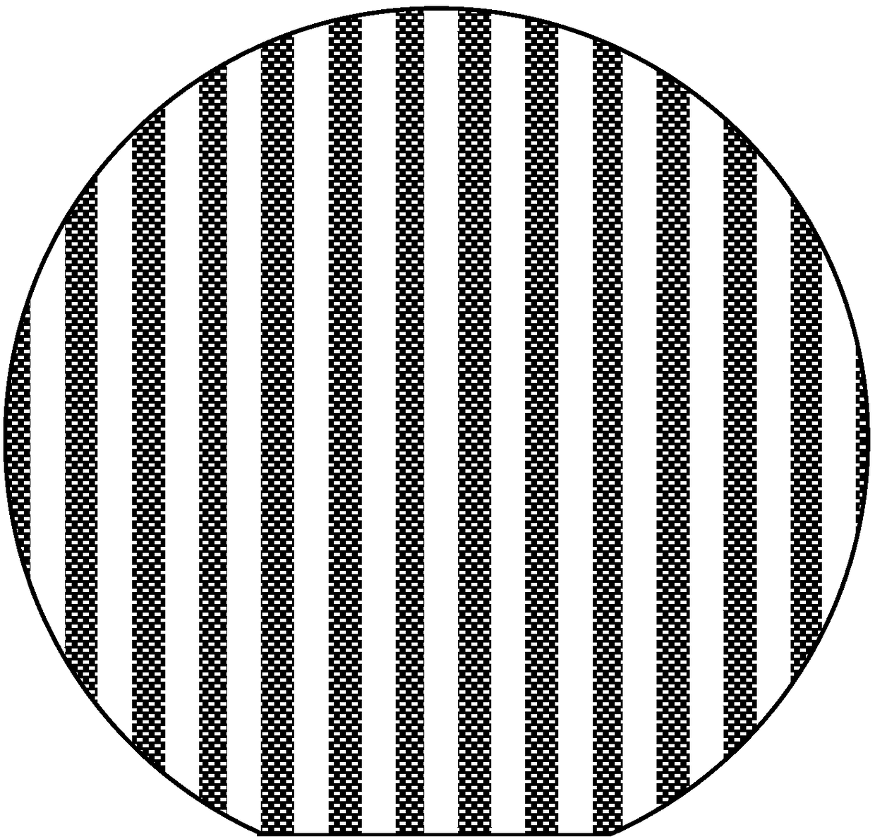
Image

Examples
Embodiment 1
[0037] Example 1, preparing a 3-inch AlN buried insulating layer uniaxially strained GeOI wafer material.
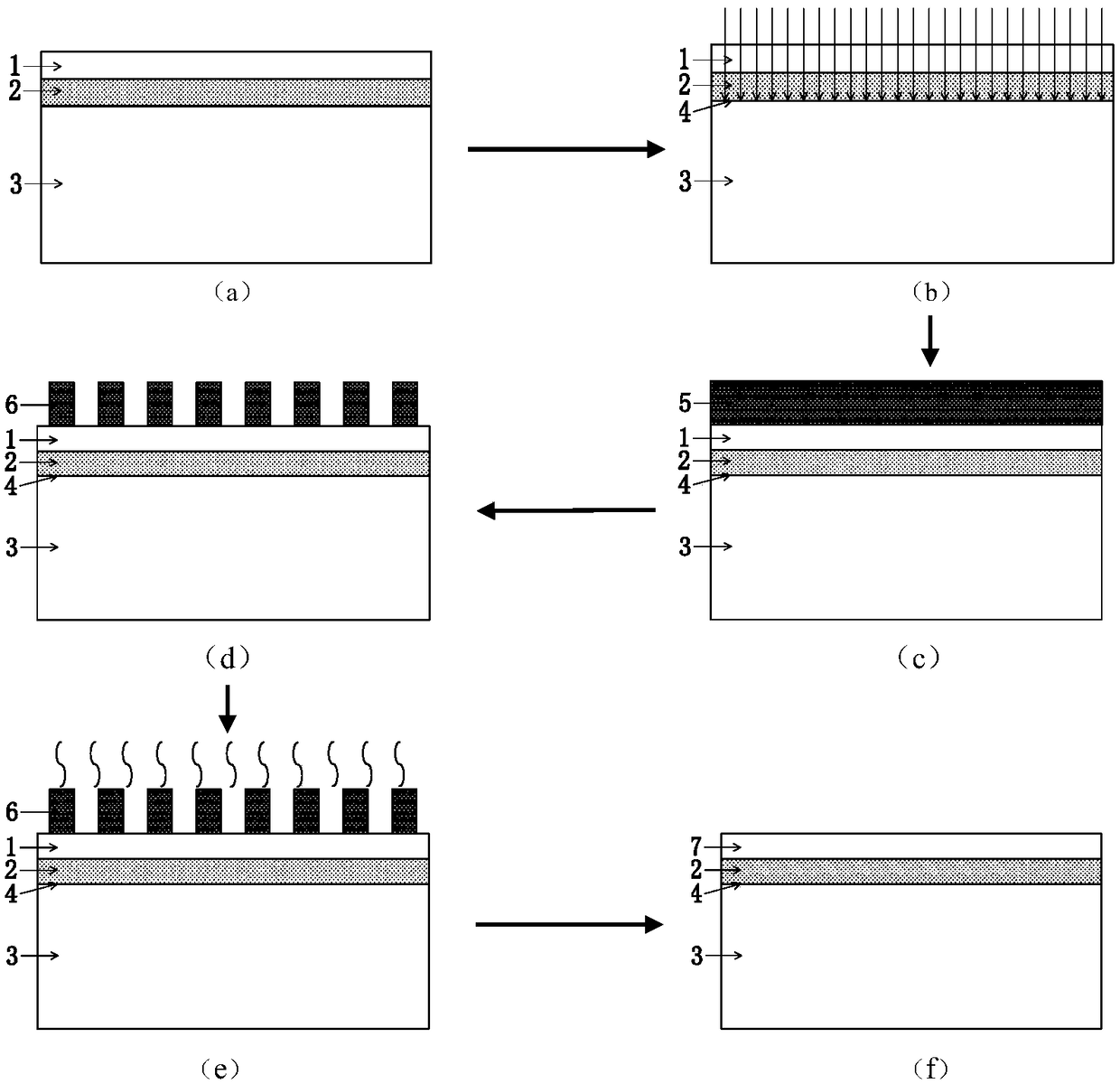
[0038] Step 1: Clean the AlN buried insulating layer GeOI wafer to remove surface pollutants.
[0039] (1.1) Use acetone and isopropanol to alternately perform ultrasonic cleaning on the GeOI wafer to remove organic contamination on the substrate surface;
[0040] (1.2) Prepare a 1:1:3 mixed solution of ammonia, hydrogen peroxide, and deionized water, and heat it to 120°C. Place the GeOI wafer in the mixed solution for 12 minutes, take it out and rinse it with a large amount of deionized water. To remove inorganic pollutants on the surface of GeOI wafers;
[0041] (1.3) Soak the GeOI wafer in HF acid buffer for 2 minutes to remove the oxide layer on the surface.
[0042] Step 2: Ion implantation.
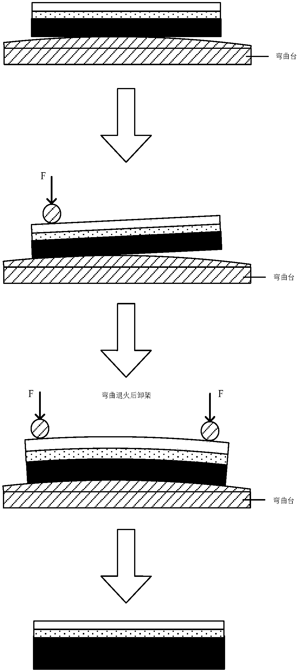
[0043] Ion implantation is carried out to the cleaned GeOI wafer, so that the interface 4 of the Si substrate 3 and the AlN buried insulating layer 2 is loose, such as fi...
Embodiment 2
[0056] Example 2, preparing a 5-inch AlN buried insulating layer uniaxially compressively strained GeOI wafer material.
[0057] Step 1: cleaning the AlN buried insulating layer GeOI wafer to remove surface pollutants.
[0058] The implementation of this step is the same as step 1 of Embodiment 1.
[0059] Step 2: Implant the cleaned GeOI wafer with a dose of 1.5E15cm -2 , He ions with an energy of 120Kev to loosen the interface 4 between the Si substrate 3 and the AlN buried insulating layer 2, such as figure 2 as shown in b.
[0060] Step 3: using the PECVD plasma enhanced chemical vapor deposition process, deposit a tensile stress SiN film 5 with a thickness of 0.9 μm and a stress of 1 GPa on the surface of the top Ge layer 1 of the ion-implanted GeOI wafer, such as figure 2 as shown in c.
[0061] The deposition process conditions are: high-frequency HF power is 1.1KW, low-frequency LF power is 0.29KW, high-purity SiH 4 The flow rate is 0.29slm, high-purity NH 3 Th...
Embodiment 3
[0070] Example 3, preparing an 8-inch AlN buried insulating layer uniaxially strained GeOI wafer material.
[0071] Step A: cleaning the AlN buried insulating layer GeOI wafer to remove surface pollutants.
[0072] The implementation of this step is the same as step 1 of Embodiment 1.
[0073] Step B: Ion implantation.
[0074] A dose of 1.5E16cm was applied to the cleaned GeOI wafer -2 , He ion implantation with an energy of 160Kev to loosen the interface 4 between the Si substrate 3 and the AlN buried insulating layer 2, such as figure 2 as shown in b.
[0075] Step C: Depositing a SiN film under high pressure stress.
[0076] PECVD plasma-enhanced chemical vapor deposition process is used to deposit a compressive stress SiN film 5 with a thickness of 1.3 μm and a stress of -1.2 GPa on the surface of the top Ge layer 1 of the GeOI wafer after ion implantation, such as figure 2 as shown in c.
[0077] The deposition process conditions are: high-frequency HF power is 0...
PUM
| Property | Measurement | Unit |
|---|---|---|
| thickness | aaaaa | aaaaa |
| width | aaaaa | aaaaa |
Abstract
Description
Claims
Application Information
 - R&D
- Intellectual Property
- Life Sciences
- Materials
- Tech Scout
- Unparalleled Data Quality
- Higher Quality Content
- 60% Fewer Hallucinations
Browse by: Latest US Patents, China's latest patents, Technical Efficacy Thesaurus, Application Domain, Technology Topic, Popular Technical Reports.
© 2025 PatSnap. All rights reserved.Legal|Privacy policy|Modern Slavery Act Transparency Statement|Sitemap|About US| Contact US: help@patsnap.com