
Light emitting diode load board and manufacturing process thereof

A technology of light-emitting diodes and manufacturing methods, applied in printed circuit manufacturing, pattern and photolithography, printed circuits, etc., to achieve the effects of increasing efficiency, improving thermal conductivity, and increasing thermal conductivity

Inactive Publication Date: 2016-10-26
TM TECHNOLOGY INC
View PDF4 Cites 3 Cited by
  • Summary
  • Abstract
  • Description
  • Claims
  • Application Information

AI Technical Summary

Problems solved by technology

[0004] In view of the above, the purpose of the present invention is to disclose a light emitting diode carrier and its manufacturing method, so as to improve the thermal conductivity of the light emitting diode carrier when manufacturing the light emitting diode carrier, and solve the alignment between the light emitting diode and the carrier Contiguous question

Method used


Image

  • Light emitting diode load board and manufacturing process thereof
  • Light emitting diode load board and manufacturing process thereof
  • Light emitting diode load board and manufacturing process thereof

Examples


Embodiment Construction

[0056] The detailed features of the present invention are described in the following embodiments, which are sufficient to enable any person familiar with the relevant art to understand the technical content of the present invention and implement it accordingly. Those skilled in the art can easily understand the related objects and advantages of the present invention. The following examples further illustrate various aspects of the present invention, but do not limit the scope of the present invention in any aspect.

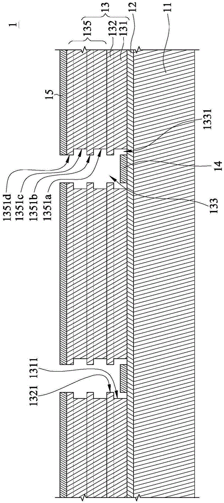
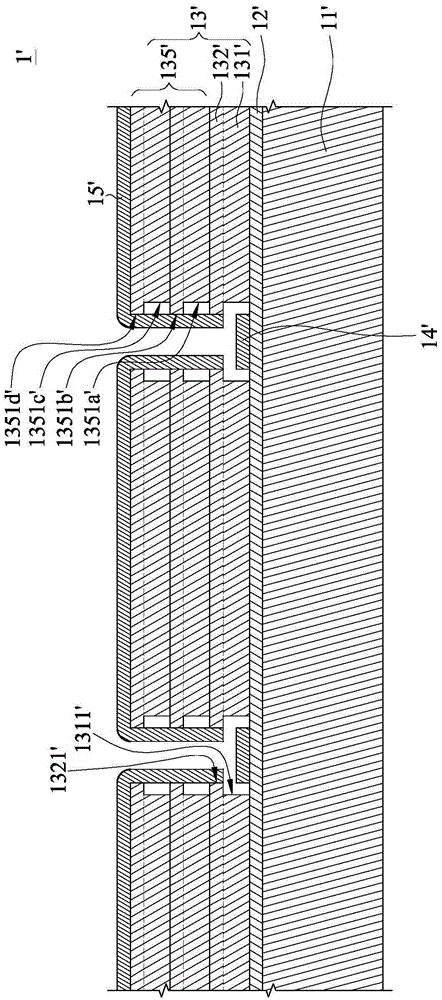
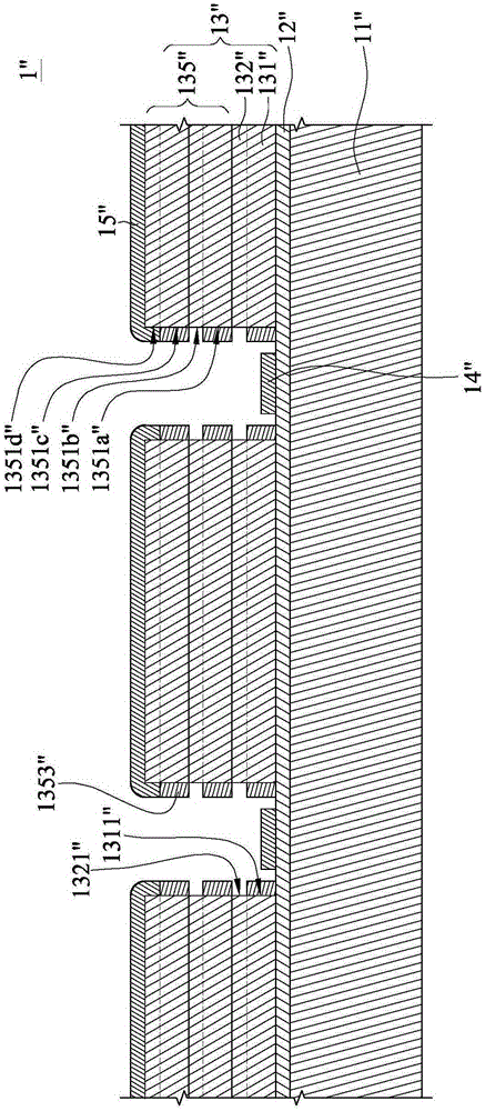
[0057] Please refer to Figure 1A , Figure 1A A schematic structural diagram of a light emitting diode carrier in an embodiment of the present invention. Such as Figure 1AAs shown, the LED carrier 1 includes a substrate 11 , a first dielectric layer 12 , a second dielectric layer 13 , a first conductive pad 14 and a second conductive pad 15 . The second dielectric layer 13 includes a first structure part 131 , a second structure part 132 and a third structure p...


PUM


Abstract

Disclosed are a light emitting diode load board and a manufacturing process thereof. The light emitting diode load board includes a substrate, a first dielectric layer, a second dielectric layer, a first conductive pad and a second conductive pad. The second dielectric layer includes a first structure part, a second structure part and a third structure part. The first dielectric layer is disposed on the substrate. The first structure part is disposed on the first dielectric layer and has a first sidewall. The second structure part is disposed on the first structure part and has a second sidewall. The third structure part is disposed on the second structure part and has N sidewalls. The second sidewall is more prominent than the first sidewall. The first sidewall, the second sidewall and the N sidewalls define the first etched part, and the part of the first dielectric layer is exposed from the first etched part. The first conductive pad is disposed in the first etched part. The second conductive is disposed on the second dielectric layer, covers part of the second dielectric and exposes the open of the first etched part.

Description

technical field [0001] The invention relates to a light-emitting diode carrier board and a manufacturing method thereof, in particular to a light-emitting diode carrier board with a calibration alignment structure and a manufacturing method thereof. Background technique [0002] Generally speaking, when a light-emitting diode is turned on to emit light, because all the electric energy cannot be used to emit light, a part of the electric energy will form heat energy. In practice, the luminous efficiency of light-emitting diodes will drop sharply due to the influence of high temperature, so more heat will be generated in addition to wasting electricity, which will further increase the temperature and cause a vicious circle. Therefore, the light-emitting diodes need to be carried on a carrier board with good heat dissipation performance, so as to avoid wasting power and shortening the lifespan. [0003] In addition, for the convenience of manufacturing, the general LED carrier...

Claims


Application Information

Patent Timeline
Patent Type & Authority Applications(China)
IPC IPC(8): H01L33/62H01L33/64H01L33/00
CPCH01L33/005H01L33/62H01L33/641H01L2933/0066H01L2933/0075H01L33/64H01L2224/16225H05K2201/0187H05K2201/0195H05K3/4007H05K1/0298H05K1/09H05K1/111H05K3/0017H05K3/4644H05K2201/09036H05K2201/10106H05K2201/10242H05K2203/0562
Inventor 吴炳松苏文铎
Owner TM TECHNOLOGY INC
Learn More