To-be-stamped structure, stamping method and product formed through method
A technology for stamping and products, applied in the field of mechanical processing, can solve the problems of high cost, long delivery cycle, short delivery cycle, etc., and achieve the effect of avoiding high cost
- Summary
- Abstract
- Description
- Claims
- Application Information
AI Technical Summary
Problems solved by technology
Method used
Image
Examples
Embodiment Construction
[0030] The present application will be further described in detail below through specific embodiments in conjunction with the drawings. The "front", "rear", "left", "right", "upper", and "lower" mentioned in the text refer to the structure to be punched and the placement state of the product formed by the punching method in the drawings.
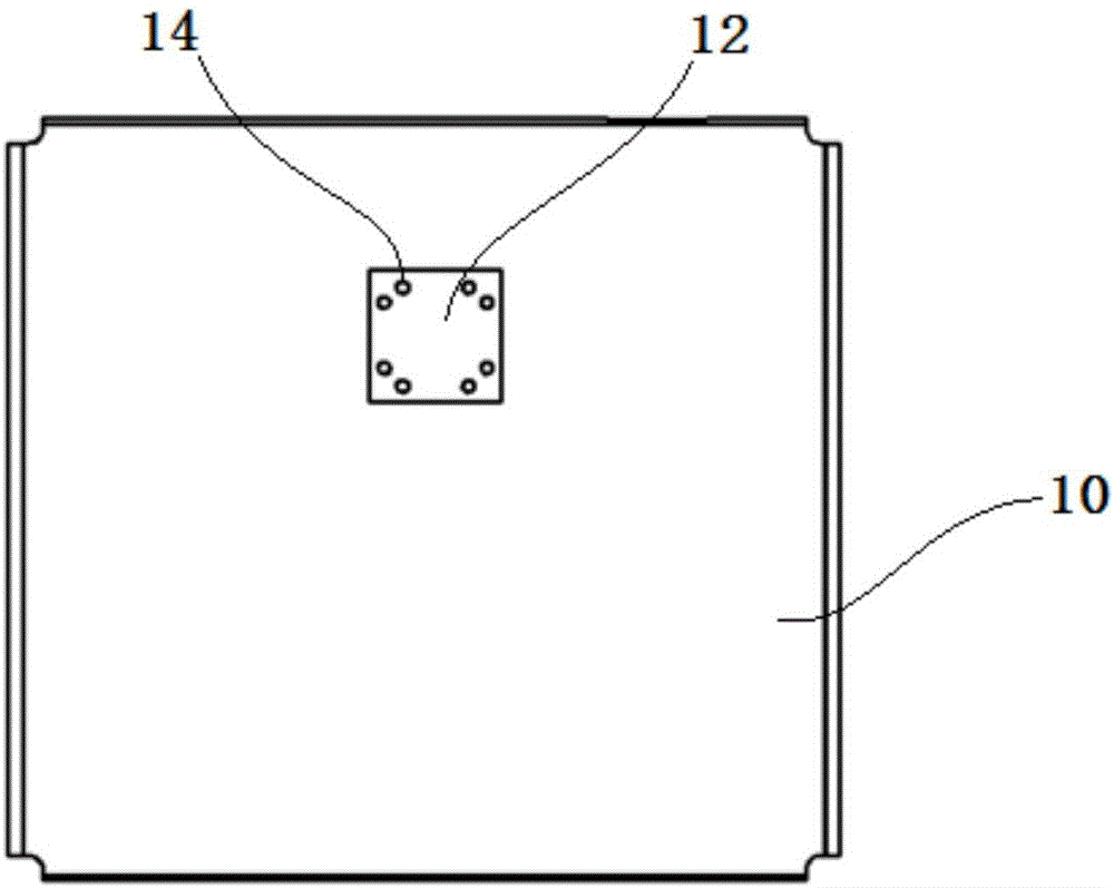
[0031] Such as figure 1 As shown, this embodiment provides a structure to be stamped, including a main body 10, a region to be thinned 12, and a material-containing cavity 14. The main body 10 constitutes a basic structure, and the region to be thinned 12 is provided on the main body 10. It is the area where the design needs to be thinned. When the stamping is completed, the thickness of the area will be smaller than other parts on the main body 10, forming a local thinning structure. The reason why the stamping process cannot form local thinning is that the stamping structures used in stamping are all solid parts, the fluidity of the material ...
PUM
| Property | Measurement | Unit |
|---|---|---|
| pore size | aaaaa | aaaaa |
| pore size | aaaaa | aaaaa |
Abstract
Description
Claims
Application Information
 - R&D
- Intellectual Property
- Life Sciences
- Materials
- Tech Scout
- Unparalleled Data Quality
- Higher Quality Content
- 60% Fewer Hallucinations
Browse by: Latest US Patents, China's latest patents, Technical Efficacy Thesaurus, Application Domain, Technology Topic, Popular Technical Reports.
© 2025 PatSnap. All rights reserved.Legal|Privacy policy|Modern Slavery Act Transparency Statement|Sitemap|About US| Contact US: help@patsnap.com


