OLED (organic light-emitting diode) display panel, display apparatus and manufacturing method for OLED display panel
A display panel and substrate technology, which is applied in semiconductor/solid-state device manufacturing, electrical components, electric solid-state devices, etc., can solve problems such as intrusion into OLED display panels, poor wettability of the first water blocking layer, and reduced lifespan of OLED display panel devices. Achieve the effect of reducing voids, increasing life, and reducing possibility
- Summary
- Abstract
- Description
- Claims
- Application Information
AI Technical Summary
Problems solved by technology
Method used
Image
Examples
Embodiment 1
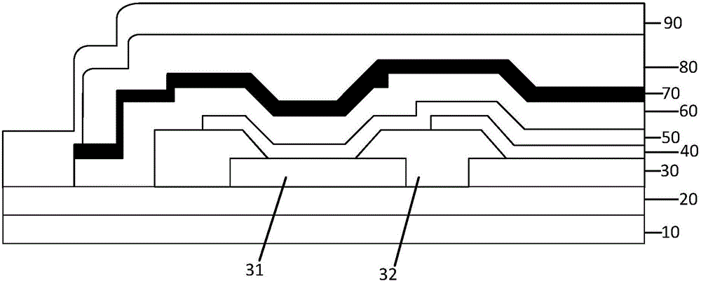
[0026] This embodiment provides an OLED display panel, figure 1 It shows a sectional view formed by cutting the OLED display panel of this embodiment in the direction of gravity when it is placed flat, and the sectional view shows a part close to the periphery of the OLED display panel, figure 1 The left side in represents the outer area of the OLED display panel.
[0027] refer to figure 1 The OLED display panel provided in this embodiment is described, the bottom of which is the substrate 10, on which a plurality of functional layers are sequentially arranged from bottom to top, and these functional layers include: an array layer (Array layer) 20, a light emitting region 30, Light emitting layer (EL layer) 40, cathode layer 50, first water blocking layer 60, organic layer 80 and second water blocking layer 60, wherein the light emitting area includes ground line (VSS line) 31 and pixel defining layer (PDL layer) 32. Wherein, the above-mentioned substrate 10 may be a fle...
Embodiment 2
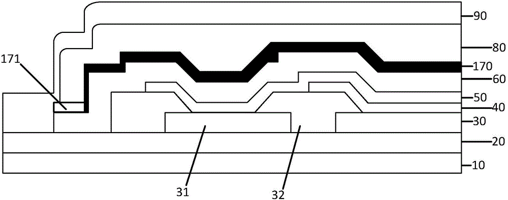
[0036] This embodiment provides an OLED display panel, figure 2 When the OLED display panel is placed flat, a cross-sectional view formed by cutting it in the direction of gravity is shown, and the cross-sectional view shows a part of the OLED display panel close to the periphery, wherein, figure 2 The left side of represents the outer area of the OLED display panel. Only the differences between the OLED display panel and the first embodiment will be described below.
[0037] In this embodiment, the first water blocking layer 60 and the organic layer 80 are the same as in Embodiment 1, and a wetting layer 170 is provided between the first water blocking layer 60 and the organic layer 80, and the wetting layer 170 The same layer is also provided with a limiting layer 171 surrounding and close to the wetting layer 170 , and the limiting layer 171 is hydrophobic.
[0038]In the prior art, in the OLED display panel, the second water blocking layer 60 covers all the functiona...
Embodiment 3
[0043] This embodiment provides a method for manufacturing an OLED display panel, which is used to manufacture the OLED display panel provided in Embodiment 1 or Embodiment 2. The method for manufacturing the OLED display panel includes:
[0044] In step S1, a wetting layer is formed on the substrate on which the first water blocking layer is formed by chemical vapor deposition or coating. This step forms a wetting layer on the first water blocking layer, wherein the material forming the wetting layer includes any one of silicon dioxide, silicon oxynitride and cationic surfactant, or any two of these substances or a combination of two or more. In addition, the above materials can also be made into an ink solution, and a wetting layer is formed on the first water blocking layer by means of inkjet printing.
[0045] Step S2, forming a thin film organic encapsulation layer on the substrate on which the wetting layer is formed. The materials for forming the organic layer are the...
PUM
 Abstract
Description
Claims
Application Information
 - R&D
- Intellectual Property
- Life Sciences
- Materials
- Tech Scout
- Unparalleled Data Quality
- Higher Quality Content
- 60% Fewer Hallucinations
Browse by: Latest US Patents, China's latest patents, Technical Efficacy Thesaurus, Application Domain, Technology Topic, Popular Technical Reports.
© 2025 PatSnap. All rights reserved.Legal|Privacy policy|Modern Slavery Act Transparency Statement|Sitemap|About US| Contact US: help@patsnap.com


