Heating device used for semiconductor fast annealing and control method

A rapid annealing and heating device technology, applied in semiconductor/solid-state device manufacturing, pulse generation, electrical components, etc., can solve the problems affecting temperature stability during the heating process, long stroboscopic period of heating lamps, and fast heating rate.

Active Publication Date: 2016-10-05
SUZHOU INST OF NANO TECH & NANO BIONICS CHINESE ACEDEMY OF SCI
View PDF5 Cites 1 Cited by
  • Summary
  • Abstract
  • Description
  • Claims
  • Application Information

AI Technical Summary

Problems solved by technology

However, due to the limitation of the dead zone of the thyristor adjustment, and in order to avoid the excessively fast heating rate during the heating process, the method of strobe flickering of the radiation lamp is generally used to achieve a stable heating rate and a constant annealing temperature in the rapid annealing process. Therefore, The inconvenience is that during the heat treatment process of the rapid annealing process, the heating lamp regulated by the thyristor has a long strobe cycle, which seriously affects the temperature stability during the heating process, and the frequent switching of the heating lamp also affects the heating lamp. tube life
In addition, in the control method of driving the thyristor to regulate the lamp tube, the PID algorithm (closed-loop control algorithm) is usually used to realize the purpose of the thyristor to regulate the lamp tube heating. This control method will inevitably introduce temperature overshoot, and the same Affects the temperature stability of the annealing process

Method used


Image

  • Heating device used for semiconductor fast annealing and control method
  • Heating device used for semiconductor fast annealing and control method
  • Heating device used for semiconductor fast annealing and control method

Examples


Embodiment Construction

[0030] In order to better describe the technical characteristics and structure of the present invention, below in conjunction with preferred embodiments of the present invention and its accompanying picture Describe in detail.

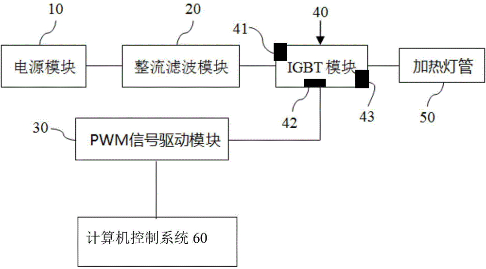
[0031] Referring to FIG. 1, a heating device for rapid annealing of semiconductors includes a power supply module 10, a rectification and filtering module 20, an IGBT (Insulated Gate Bipolar Transistor, insulated gate bipolar transistor) module 40, and a PWM (pulse width modulation) signal drive The heating lamp group 50 composed of the module 30 and several lamps includes a computer system 60 connected with the PWM signal driving module 30 for controlling and adjusting the duty cycle of the PWM signal. The power supply module 10 is connected with a rectification and filtering module 20 for providing a stable DC power supply for the heating device of this embodiment. The IGBT module 40 includes an input port 41, a control port 42, and an output port 4...


PUM


Abstract

The invention relates to a heating device used for semiconductor fast annealing and a control method. The heating device includes a power source module, a rectifying and filtering module, an IGBT (insulated gate bipolar transistor) module, a PWM (pulse width modulation) signal driving module, a heating lamp tube group and a computer control system; the power source module is connected with the rectifying and filtering module; the IGBT module comprises an input port, a control port and an output port; the rectifying and filtering module is connected with the input port of the IGBT module; the PWM signal driving module is connected with the control port of the IGBT module; the PWM signal driving module is controlled through the computer control system and is used for controlling the on-off time of the IGBT so as to adjust the heating power of the heating lamp tube group; and the heating lamp tube group is connected with the output port of the IGBT module and is used for device heating. With the heating device used for semiconductor fast annealing and the control method of the invention adopted, an overshoot phenomenon in a fast heating process can be effectively suppressed, stable temperature rise can be realized, and at the same time, the instability of heating caused by stroboflash can be avoided, and the service lives of lamp tubes can be prolonged.

Description

technical field [0001] The invention relates to the field of semiconductor manufacturing and processing, in particular to a semiconductor heat treatment process device and a heating control method. Background technique [0002] At present, the heat treatment equipment of the traditional rapid annealing process adjusts the conduction angle of the thyristor to adjust the radiation power of the lamp tube to achieve the effect of rapid temperature rise. However, due to the limitation of the dead zone of the thyristor regulation, and in order to avoid the excessively fast temperature rise rate during the heating process, the method of strobe flickering of the radiation lamp is generally used to achieve a stable temperature rise rate and a constant annealing temperature in the rapid annealing process. Therefore, The inconvenience is that during the heat treatment process of the rapid annealing process, the strobe cycle of the heating lamp regulated by the thyristor is long, which ...

Claims


Application Information

Patent Timeline
IPC IPC(8): H01L21/67H03K3/017
CPCH01L21/67098H03K3/021
Inventor 董旭崔志国熊敏李华
Owner SUZHOU INST OF NANO TECH & NANO BIONICS CHINESE ACEDEMY OF SCI
Why Eureka
Try Eureka