Chip module encapsulation structure

A packaging structure and chip module technology, applied in the field of electric power, can solve the problems of increasing production cost and increasing process, and achieve the effect of reducing production cost and simplifying the module structure

Active Publication Date: 2016-09-21
ELECTRIC POWER RESEARCH INSTITUTE, CHINA SOUTHERN POWER GRID CO LTD +1
View PDF6 Cites 5 Cited by
  • Summary
  • Abstract
  • Description
  • Claims
  • Application Information

AI Technical Summary

Problems solved by technology

[0006] In the module packaging process, the sub-module structure needs to be assembled independently, an...

Method used


Image

  • Chip module encapsulation structure
  • Chip module encapsulation structure
  • Chip module encapsulation structure

Examples


Embodiment Construction

[0064] The following will clearly and completely describe the technical solutions in the embodiments of the present invention with reference to the accompanying drawings in the embodiments of the present invention. Obviously, the described embodiments are only some, not all, embodiments of the present invention. Based on the embodiments of the present invention, all other embodiments obtained by persons of ordinary skill in the art without making creative efforts belong to the protection scope of the present invention.

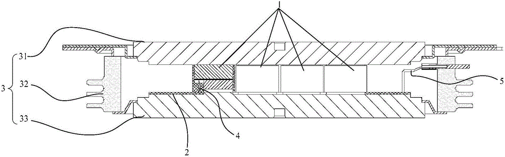
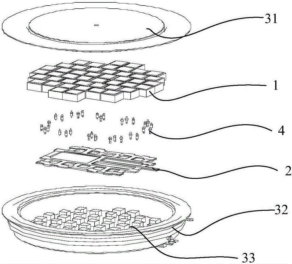
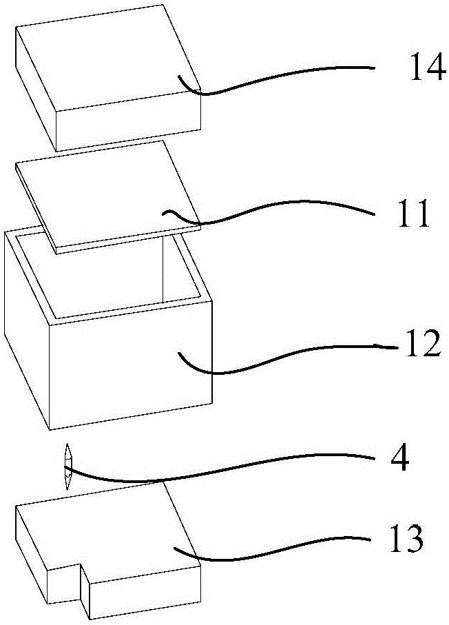
[0065] In the prior art, the typical packaging structure of the crimp-type IGBT module uses independent sub-modules. During the module packaging process, the sub-module structures need to be assembled independently and then installed on the tube socket one by one, increasing the The technological process is improved, and the production cost is increased. In order to avoid the above problems, in the chip module package structure provided by the embodiment of th...


PUM


Abstract

The embodiment of the invention provides a chip module encapsulation structure, and relates to the technical field of electric power. According to the structure, the technological process is simplified, the encapsulation time is reduced, and the production cost is reduced. The chip module encapsulation structure comprises multiple chips; a positioning element, wherein hole units which are distributed in an array are arranged on the positioning element, and each hole unit is used for fixing one chip; a shell which comprises a top shell, a middle ring and a bottom shell, wherein the edges of the top shell and the bottom shell are jointed with the upper opening and lower opening of the middle ring, multiple first molybdenum sheets are fixedly arranged on the top shell, the first molybdenum sheets correspond to the positions of the hole units, and one side of each first molybdenum sheet contacts with the first pole of each chip; and multiple bosses which are arranged on the bottom shell of the shell, wherein second molybdenum sheets are fixedly arranged on the bosses, and one side of each molybdenum sheet contacts with a second pole of each chip.

Description

technical field [0001] Embodiments of the present invention relate to the field of electric power technology, and in particular to a chip module packaging structure. Background technique [0002] The existing crimp-type IGBT (English full name, Insulated Gate Bipolar Transisitor, Chinese: Insulated Gate Bipolar Transisitor) packaging structure is usually divided into multiple units called sub-units or sub-modules according to chips. Typical IGBT module packaging structure such as figure 1 and figure 2 As shown, it includes a plurality of sub-modules 1, a PCB circuit board 2 (English full name, Printed Circuit Board, Chinese: printed circuit board) and a shell 3, and the shell 3 includes a top shell 31, a middle ring 32 and a bottom shell 33, Among them, the top shell 31 is connected to the collectors of each sub-module, the bottom shell 32 is connected to the emitters of each sub-module, the gate is connected to the PCB circuit board through the pogo pin 4, and then the c...

Claims


Application Information

Patent Timeline
IPC IPC(8): H01L25/07H01L23/04H01L23/488
CPCH01L25/072H01L23/041H01L23/488
Inventor 陈俊黎小林许树楷肖红秀窦泽春李继鲁刘国友彭勇殿
Owner ELECTRIC POWER RESEARCH INSTITUTE, CHINA SOUTHERN POWER GRID CO LTD
Why Eureka
Try Eureka