
Two-dimensional semiconductor saturable absorber mirror and preparation method thereof, and pulse fiber laser

A two-dimensional semiconductor and saturable absorption technology, applied in the field of lasers, can solve the problems of expensive SESAM, complicated manufacturing process, and narrow working bandwidth, and achieve the effects of easy preparation into products, convenient use, and high damage threshold

Inactive Publication Date: 2016-08-24
SHENZHEN UNIV
View PDF6 Cites 23 Cited by
  • Summary
  • Abstract
  • Description
  • Claims
  • Application Information

AI Technical Summary

Problems solved by technology

[0003] In order to solve the above-mentioned technical problems, the present invention provides a two-dimensional semiconductor saturable absorbing mirror and its preparation method and a pulsed fiber laser to solve the problem of high price, complex manufacturing process, low reliability and wide working bandwidth of existing commercial SESAM. narrow defect

Method used


Image

  • Two-dimensional semiconductor saturable absorber mirror and preparation method thereof, and pulse fiber laser
  • Two-dimensional semiconductor saturable absorber mirror and preparation method thereof, and pulse fiber laser
  • Two-dimensional semiconductor saturable absorber mirror and preparation method thereof, and pulse fiber laser

Examples


Embodiment Construction

[0015] In order to make the object, technical solution and advantages of the present invention clearer, the present invention will be further described in detail below in conjunction with the accompanying drawings and embodiments.

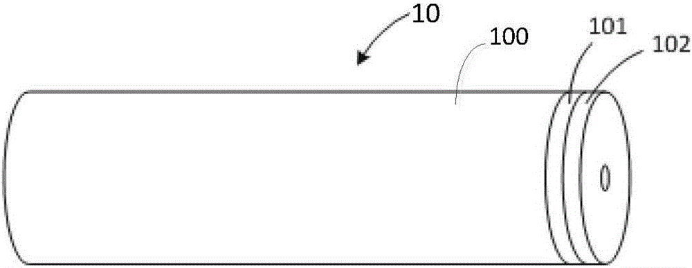
[0016] Such as figure 1 As shown, the present invention provides a two-dimensional semiconductor saturable absorber mirror 10, which includes an optical fiber 100, a two-dimensional semiconductor thin film 101 attached to the end face of the optical fiber, and a high reflection film 102 attached to the two-dimensional semiconductor thin film 101. Among them, the optical fiber can be single-mode optical fiber, polarization maintaining optical fiber, high-gain active optical fiber (such as erbium-doped optical fiber, ytterbium-doped optical fiber, thulium-doped optical fiber, holmium-doped optical fiber, praseodymium-doped optical fiber, bismuth-doped optical fiber), or active ZBLAN optical fiber .

[0017] The material of the two-dimensional semico...


PUM

PropertyMeasurementUnit
Thicknessaaaaaaaaaa

Abstract

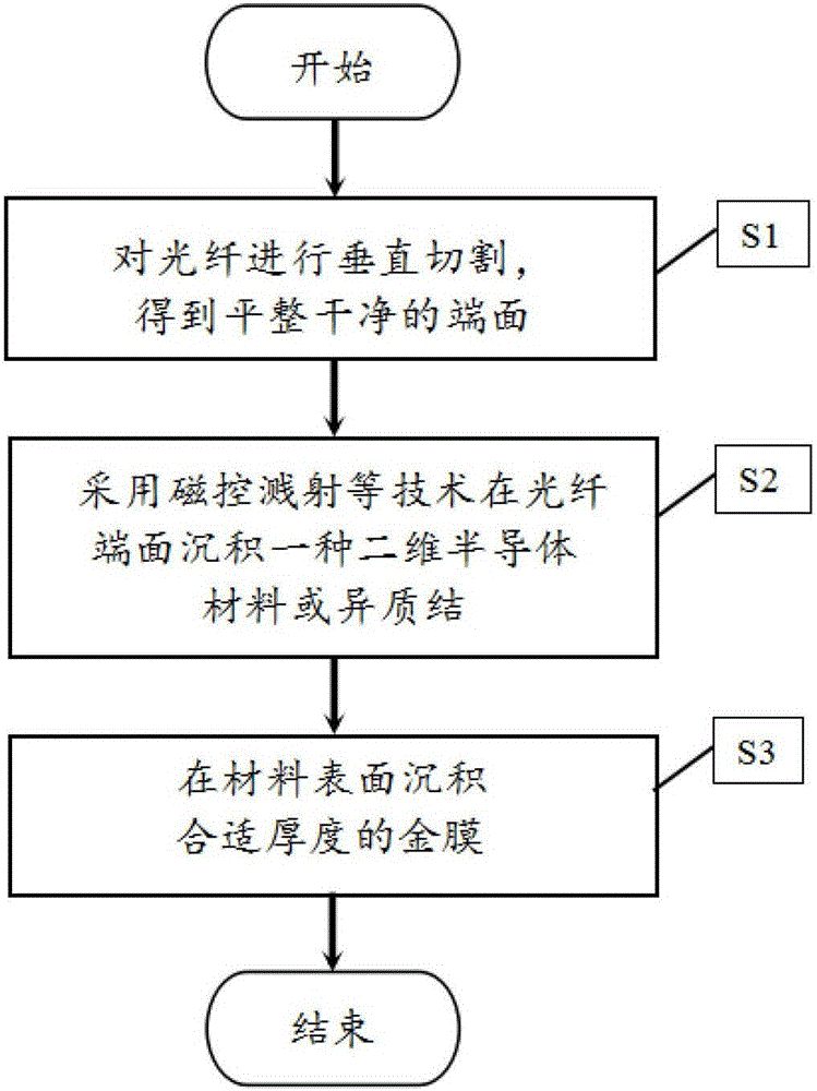
The invention relates to the technical field of lasers, and provides a two-dimensional semiconductor saturable absorber mirror. The two-dimensional semiconductor saturable absorber mirror comprises an optical fiber, a two-dimensional semiconductor film attached to the optical fiber end face and a gold film attached to the two-dimensional semiconductor film. The invention further provides a preparation method of the two-dimensional semiconductor saturable absorber mirror. The preparation method comprises the steps of: cutting the optical fiber; placing the cut optical fiber and a two-dimensional semiconductor target material in a vacuum chamber, depositing two-dimensional semiconductor plasma on the optical fiber end face, forming the two-dimensional semiconductor film, and enabling the two-dimensional semiconductor film to reach the required thickness by controlling the deposition time and / or the deposition temperature; and plating the gold film on the obtained two-dimensional semiconductor film. The novel two-dimensional semiconductor saturable absorber mirror provided by the invention is composed of the optical fiber end face, the two-dimensional semiconductor film and the gold film, and has the advantages of being high in damage threshold, simple in structure, low in cost, and high in reliability.

Description

technical field [0001] The invention belongs to the technical field of lasers, and in particular relates to a two-dimensional semiconductor saturable absorption mirror, a preparation method thereof, and a pulse fiber laser. Background technique [0002] The use of passive mode-locking technology is an effective way for fiber lasers to achieve ultrafast pulse output, and the key technology of passive mode-locking is the need for saturable absorption in the fiber laser resonator. Researchers in this field have used various saturable absorption effects to obtain passive mode-locked ultrafast pulse output in fiber lasers. In general, in order to overcome the instability of the fiber laser mode-locking environment, researchers usually use a semiconductor saturable absorber mirror (SESAM) to achieve fiber laser mode-locked ultrafast pulse output. However, commercial SESAMs are not suitable for all-round research on the dynamics of ultrafast fiber lasers due to their high price, c...

Claims


Application Information

Patent Timeline
IPC IPC(8): H01S3/098H01S3/067
CPCH01S3/1118H01S3/06708
Inventor 闫培光陈浩邢凤飞丁金妃
Owner SHENZHEN UNIV
Learn More