
GaN-based light emitting diode (LED) epitaxial structure with V-pit multi-quantum well multi-wavelength and fabrication method thereof

A multi-quantum well and epitaxial structure technology, which is applied in the direction of electrical components, circuits, semiconductor devices, etc., can solve the problem that the light source does not understand the harm of blue light, and achieve the effect of no blue light harm, simple driving circuit, and free adjustment of color rendering

Inactive Publication Date: 2016-08-17
NANCHANG UNIV +1
View PDF3 Cites 17 Cited by
  • Summary
  • Abstract
  • Description
  • Claims
  • Application Information

AI Technical Summary

Problems solved by technology

[0003] Today, when energy conservation and environmental protection are advocated, LED lighting sources have achieved unprecedented development, but the human eye health problems caused by LED lighting have not been warned in this industry, and there are relatively There are many high color temperature and low-priced low-quality products. The main reason is that manufacturers and users of LED light sources do not understand the blue light hazards produced by LED lighting.

Method used


Image

  • GaN-based light emitting diode (LED) epitaxial structure with V-pit multi-quantum well multi-wavelength and fabrication method thereof
  • GaN-based light emitting diode (LED) epitaxial structure with V-pit multi-quantum well multi-wavelength and fabrication method thereof
  • GaN-based light emitting diode (LED) epitaxial structure with V-pit multi-quantum well multi-wavelength and fabrication method thereof

Examples


Embodiment 1

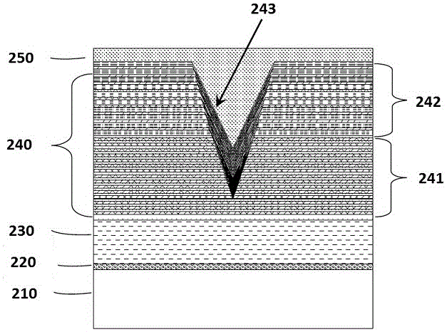
[0039] as shown in the picture 2 shown, according to the example 1 the belt V Pit Multiple Quantum Well Multiple Wavelength GaN base led The epitaxial structure includes: substrate 210 , buffer layer set on the substrate 220 , set on the buffer layern type layer 230 , set at n type layer 230 active layer on 240 and set in the active layer 240 Up P type layer 250 。

[0040] In this example, in n type layer 230 Active layer set on 240 including multiple layers 241 , Lighting unit 242 and V pit 243 。

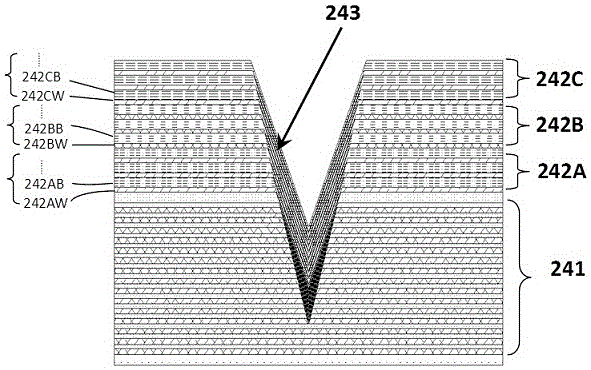
[0041] In this embodiment, as shown in 3 As shown, the light emitting unit 242 set in a multi-layer structure 241 on, including 3 luminous area 242A 、 242B and 242C , which in turn is set in a multi-layer structure 241 blue multiple quantum well light-emitting region 242A , set in the blue light multi-quantum well light-emitting area 242A Green Multiple Quantum Well Light Emitting Region 242B , set in the green...

Embodiment 2

[0045] as shown in the picture 4 shown, according to the example 2 with V Pit Multiple Quantum Well Multiple Wavelength GaN base led The epitaxial structure includes: substrate 310 , set on the substrate 310 buffer layer on 320 , set in the buffer layer 320 Up n type layer 330 , set at n type layer 330 active layer on 340 and set in the active layer 340 Up P type layer 350 。

[0046] In this example, in n type layer 330 Active layer set on 340 including multiple layers 341 , Lighting unit 342 and V pit 343 。

[0047] In this embodiment, as shown in 5 As shown, the light emitting unit 342 set in a multi-layer structure 341 on, including 4 luminous area 342A 、 342B 、 342C and 342D , which in turn is set in a multi-layer structure 341 blue multiple quantum well light-emitting region 342A , set in the blue light multi-quantum well light-emitting area 342A multi-subwell light-emitting region 342B , set in the c...

Embodiment 3

[0051] as shown in the picture 6 shown, according to the example 3 with V Pit Multiple Quantum Well Multiple Wavelength GaN base led The epitaxial structure includes: substrate 410 , buffer layer set on the substrate 420 , set on the buffer layer n type layer 430 , set at n type layer 430 active layer on 440 and set in the active layer 440 Up P type layer 450 。

[0052] In this example, in n type layer set on the active layer 440 including multiple layers 441 , Lighting unit 442 and V pit 443 。

[0053] In this embodiment, as shown in 7 As shown, the light emitting unit 442 set in a multi-layer structure 441 on, including 5 luminous area 442A 、 442B 、 442C 、 442D and 442E , which in turn is set in a multi-layer structure 441 blue multiple quantum well light-emitting region 442A , set in the blue light multi-quantum well light-emitting area 442A Cyan multiple quantum well light-emitting region 442B , set in the cy...


PUM


Abstract

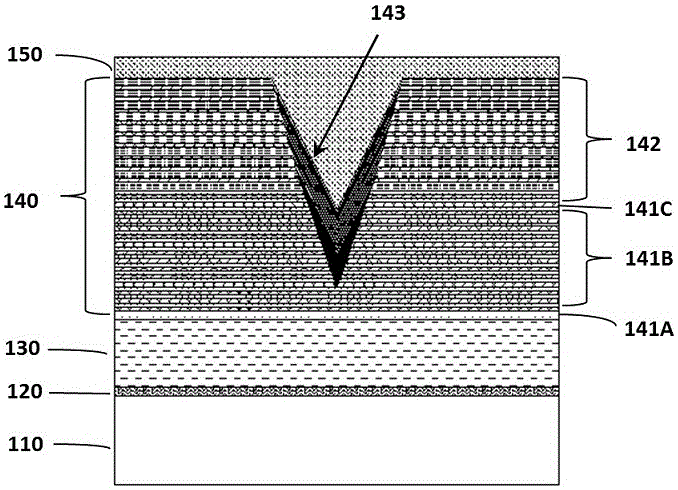
The invention discloses a GaN-based light emitting diode (LED) epitaxial structure with V-pit multi-quantum well multi-wavelength and a fabrication method thereof. The structure comprises a substrate, a buffer layer, an n-type layer, an active layer and a P-type layer, wherein the buffer layer, the n-type layer, the active layer and the P-type layer are sequentially laminated on the substrate, the active layer comprises a multi-layer structure and a luminous unit, the luminous unit comprises 3-10 multi-quantum well luminous regions emitting luminous wavelengths, the multi-layer structure exists in a V pit, and the V pit generates the multi-layer structure and passes through the multi-quantum well luminous regions. Through the GaN-based light emitting diode (LED) epitaxial structure with V-pit multi-quantum well multi-wavelength, obtained according to the method, the problems of short service lifetime of fluorescent powder, high color temperature, low color rendering index, partial harm of blue-light short-wavelength and the like existing in the conventional mainstream white-light LED can be solved, and a single-chip LED without the fluorescent powder gives out white light.

Description

technical field [0001] The invention relates to the field of semiconductor light-emitting devices, in particular to a GaN-based LED epitaxial structure with V pits, multiple quantum wells, and multiple wavelengths and a preparation method thereof. Background technique [0002] LED is called the fourth-generation lighting source or green light source. It has the characteristics of energy saving, environmental protection, long life, and small size. It can be widely used in various indications, displays, decorations, backlights, general lighting, and urban night scenes. There are usually two ways to realize white LED. The first is to use GaN-based blue LED and phosphor to form white light; the second is to use a variety of monochromatic light (blue, green, yellow, red four primary colors or five , six primary colors) mixed to form white light. [0003] Today, when energy conservation and environmental protection are advocated, LED lighting sources have achieved unprecedented d...

Claims


Application Information

Patent Timeline
Patent Type & Authority Applications(China)
IPC IPC(8): H01L33/32H01L33/08H01L33/06H01L33/00
CPCH01L33/32H01L33/0075H01L33/06H01L33/08
Inventor 莫春兰刘军林江风益全知觉张建立王小兰王光绪吴小明
Owner NANCHANG UNIV
Learn More