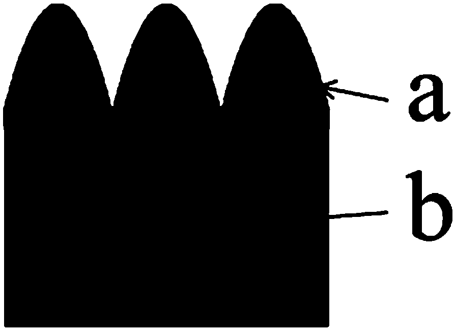
Sapphire optical performance improvement method based on micron-scale array structure and yttrium oxide thin film
An array structure and optical performance technology, applied in ion implantation plating, metal material coating process, coating and other directions, can solve the problems of few film selection, difficult matching, complex surface microstructure treatment design, etc. cost effect
- Summary
- Abstract
- Description
- Claims
- Application Information
AI Technical Summary
Problems solved by technology
Method used
Image
Examples
Embodiment 1
[0019] The diameter of the bottom surface of the cone is 2.6 μm, the period is 0.4 μm, and the heights are 1.2 μm, 1.4 μm and 1.6 μm respectively. The preparation parameters of yttrium oxide: power 150W, sputtering pressure 2Pa, oxygen flow 3sccm, argon flow 30sccm, thickness 200nm, 350℃ Insulation annealing in air for 2h. The average optical properties of the measured sapphire in the 3-5 μm mid-infrared band are shown in Table 1.
[0020] Table 1 Effects of different microstructure heights on the optical properties of sapphire
[0021] Cone height / μm
Embodiment 2
[0023] Conical bottom diameter 2.6μm, period 0.4μm, height 1.6μm, yttrium oxide preparation parameters: power 150W, sputtering pressure 2Pa, oxygen flow rate 3sccm, argon flow rate 30sccm, heat preservation and annealing in air at 350°C for 2h, thickness of 100, 200 and Table 2 shows the average optical properties of sapphire measured at 300nm in the 3-5μm mid-infrared band.
[0024] Table 2 Effects of different film thicknesses on the optical properties of sapphire
[0025] Film thickness / nm
Embodiment 3
[0027] Conical bottom diameter 2.6μm, period 0.4μm, height 1.6μm, yttrium oxide preparation parameters: power 150W, sputtering pressure 1.0Pa, 3.0Pa and 5.0Pa, oxygen flow 3sccm, argon flow 30sccm, heat preservation and annealing in air at 350°C for 2h , with a thickness of 200nm, the average optical properties of the measured sapphire in the mid-infrared band of 3-5μm are shown in Table 3.
[0028] Table 3 Effects of different sputtering pressures on the optical properties of sapphire
[0029] Sputtering pressure / Pa
PUM
| Property | Measurement | Unit |
|---|---|---|
| diameter | aaaaa | aaaaa |
| thickness | aaaaa | aaaaa |
| diameter | aaaaa | aaaaa |
Abstract
Description
Claims
Application Information
 - R&D
- Intellectual Property
- Life Sciences
- Materials
- Tech Scout
- Unparalleled Data Quality
- Higher Quality Content
- 60% Fewer Hallucinations
Browse by: Latest US Patents, China's latest patents, Technical Efficacy Thesaurus, Application Domain, Technology Topic, Popular Technical Reports.
© 2025 PatSnap. All rights reserved.Legal|Privacy policy|Modern Slavery Act Transparency Statement|Sitemap|About US| Contact US: help@patsnap.com

