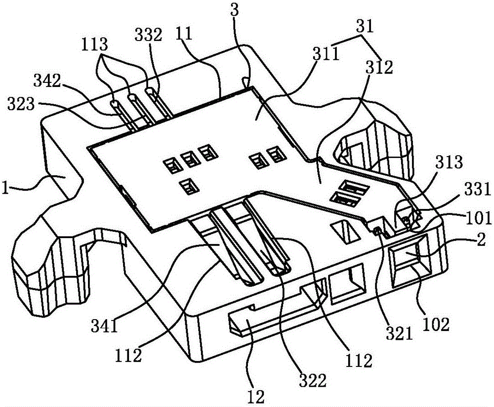
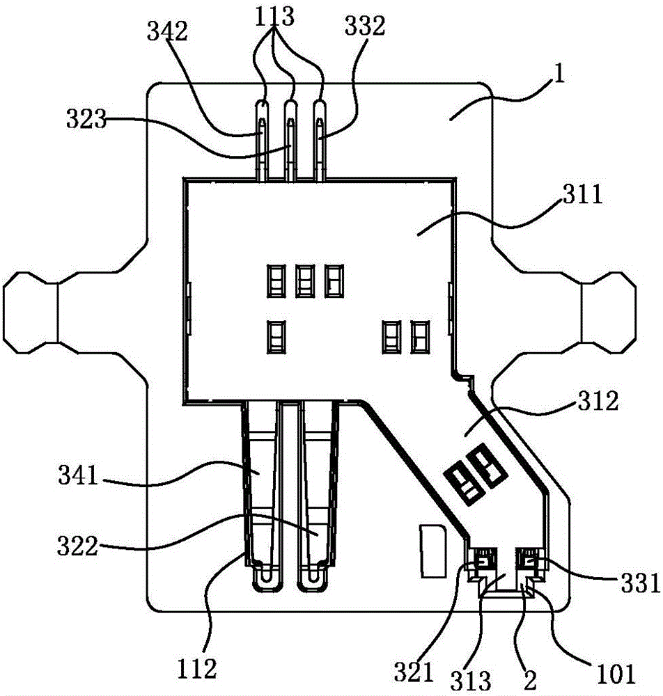
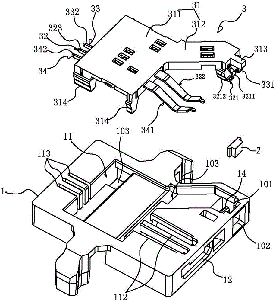
LED chip assembly structure and assembly method of smart label connector
A technology of LED chips and smart labels, which is applied to the parts of the connection device, the assembly/disassembly of the contacts, the protective grounding/shielding device of the connection parts, etc., which can solve the problems of unfavorable market competitiveness, complicated assembly process, and difficult disassembly and assembly, etc. problems, to achieve the effect of ensuring stability and communication quality, easy assembly, simplified complexity and difficulty of assembly
- Summary
- Abstract
- Description
- Claims
- Application Information
AI Technical Summary
Problems solved by technology
Method used
Image
Examples
Embodiment 2
[0081] combine Figure 13 As mentioned above, the difference between the second embodiment and the first embodiment above is that the first bending part 3212 in the first elastic contact arm 321 in the second embodiment is located at the lower end of the first raised part 3211, that is to say, The first bending part of the first elastic contact arm in the above-mentioned embodiment 1 faces upwards, while the first bending part of the first elastic contact arm of the second embodiment faces downwards, which has the same technical effect. This will not repeat them one by one.
Embodiment 3
[0083] combine Figure 14 As mentioned above, the difference between the second embodiment and the first embodiment is that the first elastic contact arm 321 includes a first raised portion 3211 formed by bending, and the first raised portion 3211 is in contact with the outer surface of the LED chip 2 The shape and structure of the elastic connecting arm 331 in the ground terminal 33 are the same as the shape and structure of the first elastic contact arm 321 . That is to say, the first elastic contact arm 321 and the elastic lead arm 331 of the ground terminal are respectively clamped on the two sides of the LED chip 2, and are elastically connected to the positive and negative electrodes 21 and 22 on the two sides of the LED chip 2 respectively. contact and form a non-soldering conduction.
[0084] Except for the above, the other structures of the third embodiment are the same as those of the first embodiment above, and have basically the same technical effects, and will no...
Embodiment 4
[0086] combine Figure 15 As mentioned above, the difference between the fourth embodiment and the first embodiment above is that the first elastic contact arm 321 includes a first raised portion 3211 formed by bending, and the first raised portion 3211 is connected to the front end of the LED chip 2 The shape and structure of the elastic contact arm 331 in the ground terminal 3 are the same as the shape and structure of the first elastic contact arm 321 . That is to say, the first elastic contact arm 321 and the elastic guide arm 331 are respectively in contact with the two ends of the front end of the LED chip 2, and the rear end of the LED chip 2 is in contact with the end of the extension seat 312, so that the first elastic contact arm 321 and the elastic connecting arm 331 can respectively form a stable elastic contact with the positive and negative electrodes 21 and 22 on the front surface of the LED chip 2, and form a non-welding conduction.
[0087] Except for the abo...
PUM
 Abstract
Description
Claims
Application Information
 - R&D Engineer
- R&D Manager
- IP Professional
- Industry Leading Data Capabilities
- Powerful AI technology
- Patent DNA Extraction
Browse by: Latest US Patents, China's latest patents, Technical Efficacy Thesaurus, Application Domain, Technology Topic, Popular Technical Reports.
© 2024 PatSnap. All rights reserved.Legal|Privacy policy|Modern Slavery Act Transparency Statement|Sitemap|About US| Contact US: help@patsnap.com


