
Impedance matching method for plasma processing device

A processing device and impedance matching technology, applied in semiconductor/solid-state device manufacturing, discharge tubes, electrical components, etc., can solve the problems of poor plasma treatment process uniformity, poor uniformity of plasma distribution density, etc.

Active Publication Date: 2016-07-27
ADVANCED MICRO FAB EQUIP INC CHINA
View PDF6 Cites 4 Cited by
  • Summary
  • Abstract
  • Description
  • Claims
  • Application Information

AI Technical Summary

Problems solved by technology

[0004] However, the existing impedance matching method will cause poor uniformity of plasma distribution density during plasma treatment, resulting in poor uniformity of plasma treatment process

Method used


Image

  • Impedance matching method for plasma processing device
  • Impedance matching method for plasma processing device
  • Impedance matching method for plasma processing device

Examples


Embodiment Construction

[0039] As mentioned in the background art, the existing impedance matching method will result in poor uniformity of plasma distribution density in the plasma treatment process, resulting in poor uniformity of the plasma treatment process.

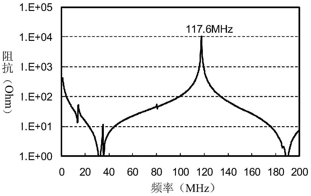
[0040] After research, it is found that in the case of fixed external matching network parameters, only adjusting the output frequency of the RF power supply has the following advantages: figure 1 The frequency characteristics shown. A reaction chamber for performing a plasma treatment process generally has an eigenfrequency, and in a range around the eigenfrequency, the impedance of the reaction chamber increases sharply, specifically as figure 1 as shown, figure 1 It is a schematic diagram of the relationship between the frequency and the blocking of the reaction chamber.

[0041] Please refer to figure 1 , when the frequency is 117.6 MHz, the impedance of the reaction chamber reaches a peak value of 10000 ohms, therefore, the frequenc...


PUM


Abstract

An impedance matching method for a plasma processing device is disclosed. The method comprises the following steps: the impedance matching device is connected between a plasma processing device and a variable frequency power source; the impedance matching method comprises the variable frequency power source, a first variable capacitor, a second variable capacitor and an electric inductor; a resonant frequency scope of the plasma processing device is obtained; the impedance matching device enters a frequency adjusting mode which comprises a plurality of frequency adjusting steps; an output frequency of the variable frequency power source in a next step is obtained; if the output frequency in the next step is not in the resonant frequency scope, loop execution the frequency adjusting steps is carried out till impedance matching is realized; if the output frequency in the next step is in the resonant frequency scope, the frequency adjusting mode is halted, and the impedance matching device enters a capacitance adjusting step; the first variable capacitor is adjusted according to currently detected reflection power signals of the plasma processing device. The impedance matching method for the plasma processing device enables state stability of plasmas, plasma processing quality improvement, and plasma processing state stability.

Description

technical field [0001] The invention relates to the technical field of semiconductor manufacturing, in particular to an impedance matching method of a plasma processing device. Background technique [0002] Plasma treatment processes used in the manufacture of integrated circuits include plasma deposition processes, plasma etching processes, and the like. The principle of the plasma treatment process includes: using a radio frequency power source to drive a plasma generating device (such as an inductively coupled coil) to generate a strong high frequency alternating magnetic field, so that a low pressure reaction gas is ionized to generate plasma. Plasma contains a large number of active particles such as electrons, ions, excited atoms, molecules and free radicals, which can undergo various physical and chemical reactions with the surface of the wafer to be processed, making the morphology of the wafer surface changes occur, ie the plasma treatment process is complete. [...

Claims


Application Information

Patent Timeline
IPC IPC(8): H01J37/32H01L21/02
Inventor 叶如彬梁洁
Owner ADVANCED MICRO FAB EQUIP INC CHINA
Learn More