Class superlattice tin-selenium/antimony nanometer phase transition film, and preparation and application thereof
A technology similar to superlattice tin and superlattice, applied in the field of microelectronic materials, can solve the problems that affect the reliability and cycle life of PCRAM devices, phase change materials are not suitable for PCRAM devices, and poor contact between phase change layers and devices, etc. The effect of high reliability, fast phase change speed and low programming power consumption
- Summary
- Abstract
- Description
- Claims
- Application Information
AI Technical Summary
Problems solved by technology
Method used
Image
Examples
Embodiment 1
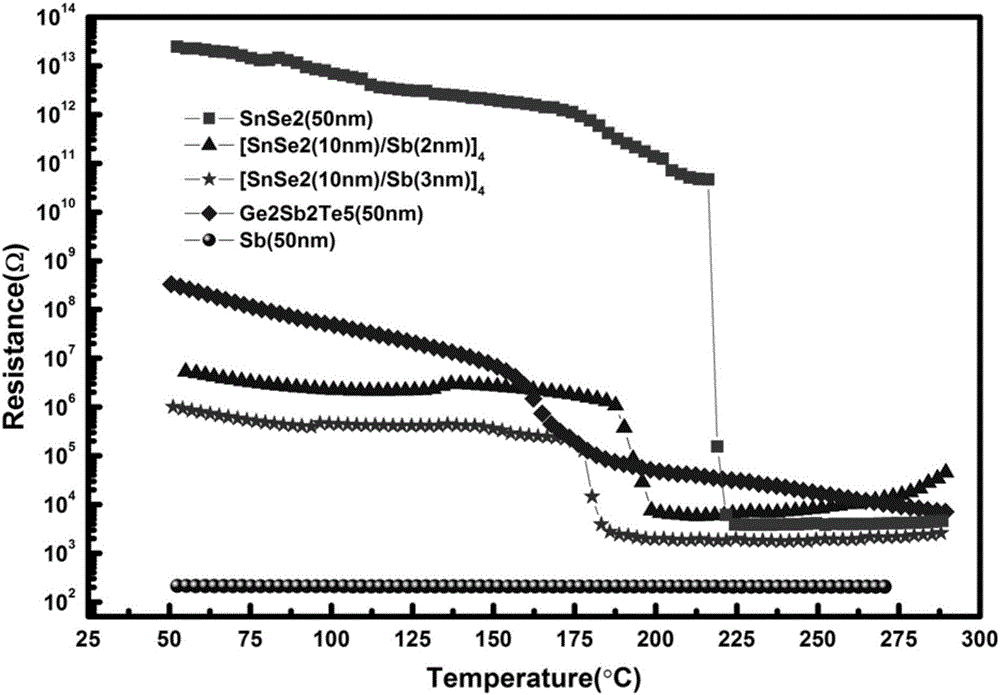
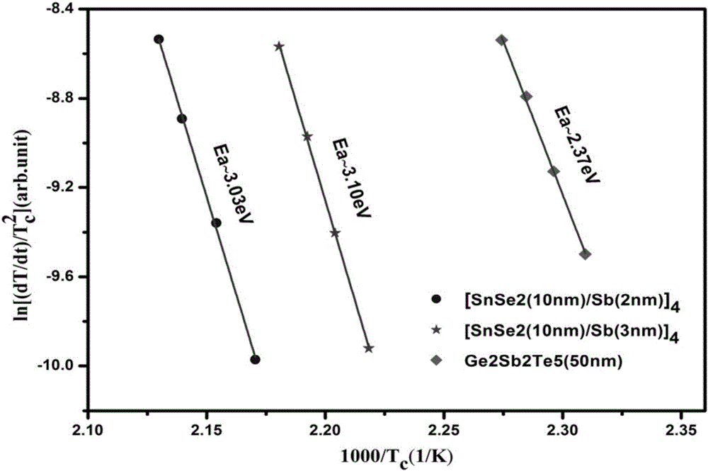
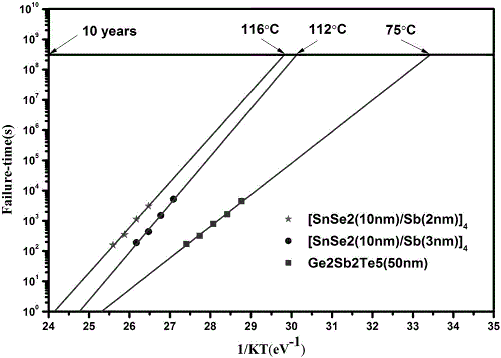
[0036] A superlattice-like tin-selenium / antimony nano phase change film, the phase change film comprising SnSe 2 Material and elemental Sb material, the two films form a superlattice-like structure through multi-layer nanocomposite, and the general structure of the phase change film is [SnSe 2 (10nm) / Sb(2nm)) 4 , Where the SnSe in each phase change film 2 The thickness of the material is 10 nm, the thickness of the elemental Sb material in each phase change film is 2 nm, and the number of periods of the phase change film is 4 layers.
[0037] The preparation method of the phase change film mainly includes the following steps:
[0038] 1. Cleaning SiO 2 / Si(100) substrate surface and back, to remove dust particles, organic and inorganic impurities:
[0039] (a) Place the substrate in an ethanol solution and clean it with ultrasonic for 20 minutes to remove dust particles and inorganic impurities on the surface of the substrate;
[0040] (b) Put the substrate in an acetone solution and c...
Embodiment 2
[0054] Using the same preparation method as in Example 1, the difference is:
[0055] Rotate the substrate to the Sb target position (target position 1), turn on the DC sputtering power supply, and sputter 2.143s to form a 3nm Sb film;
[0056] Therefore, the general formula of the final phase change film is [SnSe 2 (10nm) / Sb(3nm)) 4 .
Embodiment 3
[0073] A superlattice-like tin-selenium / antimony nano phase change film, the phase change film comprising SnSe 2 Material and elemental Sb material, the two films form a superlattice-like structure through multi-layer nanocomposite. The general structure of the phase change film is [SnSe 2 (8nm) / Sb(1.5nm)) 5 , Where the SnSe in each phase change film 2 The thickness of the material is 8 nm, the thickness of the elemental Sb material in each phase change film is 1.5 nm, and the period of the phase change film is 5, so the total thickness of the phase change film is 47.5 nm.
[0074] The preparation method of the phase change film mainly includes the following steps:
[0075] 1. Cleaning SiO 2 / Si(100) substrate surface and back, to remove dust particles, organic and inorganic impurities:
[0076] (a) Put the substrate in an ethanol solution and clean it with ultrasonic for 15 minutes to remove dust particles and inorganic impurities on the surface of the substrate;
[0077] (b) Put the ...
PUM
| Property | Measurement | Unit |
|---|---|---|
| crystallization temperature | aaaaa | aaaaa |
| thickness | aaaaa | aaaaa |
| phase transition temperature | aaaaa | aaaaa |
Abstract
Description
Claims
Application Information
 - R&D
- Intellectual Property
- Life Sciences
- Materials
- Tech Scout
- Unparalleled Data Quality
- Higher Quality Content
- 60% Fewer Hallucinations
Browse by: Latest US Patents, China's latest patents, Technical Efficacy Thesaurus, Application Domain, Technology Topic, Popular Technical Reports.
© 2025 PatSnap. All rights reserved.Legal|Privacy policy|Modern Slavery Act Transparency Statement|Sitemap|About US| Contact US: help@patsnap.com


