
Fast recovery diode material slice structure containing cathode auxiliary part and manufacturing method thereof

A technology for recovering diodes and auxiliary structures, which is applied in the direction of electrical components, circuits, semiconductor devices, etc., and can solve the problems of short recombination time, long transition zone, and high cost of epitaxial wafers

Inactive Publication Date: 2016-07-13
上海芯石微电子有限公司
View PDF6 Cites 3 Cited by
  • Summary
  • Abstract
  • Description
  • Claims
  • Application Information

AI Technical Summary

Problems solved by technology

[0003] Fast recovery diodes generally use three-spread sheets and epitaxial sheets as substrates. Common fast-recovery diode substrates use three-spread sheets. The cathode of this material sheet is usually formed by deep diffusion of phosphorus to act as a buffer layer. This design leads to N+ The transition region is long, the conduction voltage drop will increase, the recombination time will be long, and the reverse recovery time will be long; the high-efficiency fast recovery diode substrate adopts epitaxial wafers, the substrate doping concentration is very high, and the concentration gradient near the contact with the epitaxial layer is very steep , so the reverse recovery time of the product is much shorter than that of ordinary fast recovery diodes, the voltage drop is also much smaller, the recombination time is short, and the reverse recovery time is short, but the epitaxial wafers are manufactured with expensive equipment, so the cost of the epitaxial wafers is high

Method used


Image

  • Fast recovery diode material slice structure containing cathode auxiliary part and manufacturing method thereof
  • Fast recovery diode material slice structure containing cathode auxiliary part and manufacturing method thereof

Examples


Embodiment

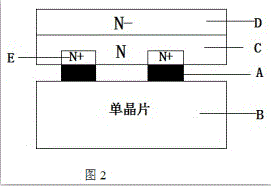
[0012] Such as figure 2 , Diffusion of phosphorus (1260°C, 2h) on the back of a low-doped N-monocrystalline silicon wafer (thickness 260um) to form an N-type region (C), with a junction depth of 20um, and then use the screen printing process, the screen uses 800 mesh For processing, the scraper uses a rubber knife, the scraper pressure is 3kg, the scraper speed is 70mm / s, and a layer of phosphorus latex source (A) is coated on the surface of the N area (C), with a viscosity of about 150CP, baked on a hot plate at 200°C for 1min, After baking, the thickness of the latex source is 20um, and the width is 100um. A single wafer (B) is adhered to the coated surface of the silicon wafer (A), and the two adhered silicon wafers are diffused at a high temperature of 1200°C to form dot-shaped N+ Area (E), N+ junction depth at 5um, surface concentration at 1E19 / cm 2 Above, the N+ area (E) and the N area (C) form the auxiliary part of the cathode. After the furnace is released, the front...


PUM

PropertyMeasurementUnit
Thicknessaaaaaaaaaa

Abstract

The invention mainly aims to provide a fast recovery diode material slice structure containing a cathode auxiliary part. High-concentration N+ junctions are arranged at intervals and manufactured on the N surface of an N type monocrystalline wafer, and the fast recovery diode material slice structure has a self-modulation effect and has good soft recovery characteristics; according to the material slice, the monocrystalline wafer adheres to the N surface in a silicon oxidation mode, and the wafer is not fragile in the processing process. The manufacturing cost of the structure is lower than that of an epitaxial slice. Compared with the conventional processed epitaxial slice, the fast recovery diode material slice structure containing the cathode auxiliary part has good fast and soft recovery characteristics and is lower in cost.

Description

technical field [0001] The invention belongs to the technical field of diode material sheet preparation, in particular to a cathode-assisted fast recovery diode material sheet structure and a manufacturing method thereof. Background technique [0002] In electronic circuits, diodes are one of the most commonly used basic electronic components; in power electronic circuits, diodes go hand in hand with switching devices and are indispensable; in many cases, the number of diodes in power electronic circuits is more than that of switching devices , plays a pivotal role in the circuit, especially the requirements for high-power diodes used in matching with switching devices are the most special, but higher requirements are put forward for high-power switching diodes used in the circuit, the faster the reverse recovery time, the better , the reverse recovery time is determined by the substrate concentration. The existence of the substrate doping concentration gradient increases th...

Claims


Application Information

Patent Timeline
IPC IPC(8): H01L29/02H01L29/868
CPCH01L29/02H01L29/868
Inventor 王国峰
Owner 上海芯石微电子有限公司
Learn More