Liquid crystal display element
A technology for liquid crystal display elements and liquid crystal layers, applied in the directions of liquid crystal materials, instruments, chemical instruments and methods, can solve the problems of white spots and uneven orientation, and achieve the effect of preventing white spots and preventing decline.
- Summary
- Abstract
- Description
- Claims
- Application Information
AI Technical Summary
Problems solved by technology
Method used
Image
Examples
no. 1 approach >
[0038] A first preferred embodiment of the liquid crystal display element according to the present invention has a thin film transistor using an oxide semiconductor and a specific liquid crystal composition, and generates an electric field in a substantially vertical direction between the first substrate and the second substrate of the liquid crystal display element. Liquid crystal display element. The first preferred embodiment is a liquid crystal display element having electrodes on a first substrate and a second substrate, for example, a transmissive liquid crystal display element using a VA (Vertical Alignment: Vertical Alignment) type.
[0039] The first preferred embodiment of the liquid crystal display element according to the present invention preferably has a first substrate and a second substrate arranged to face each other, and a liquid crystal layer containing a liquid crystal composition is sandwiched between the first substrate and the second substrate, It also h...
no. 2 approach >
[0251] The second embodiment of the liquid crystal display element according to the present invention is a liquid crystal display element having a thin film transistor using an oxide semiconductor and a specific liquid crystal composition, and generating an electric field having a component parallel to the substrate surface of the liquid crystal display element. . The second preferred embodiment is an IPS type liquid crystal display element (In Plane Switching mode Liquid Crystal Display) or an FFS type liquid crystal display element (Fringe Field Switching mode Liquid Crystal Display element (Fringe Field Switching mode Liquid Crystal Display element) as a kind of IPS type liquid crystal display element. Crystal Display).
[0252] An IPS type liquid crystal display element which is a second preferred embodiment of the liquid crystal display element according to the present invention has a first substrate and a second substrate arranged to face each other, and a substrate cont...
no. 3 approach >
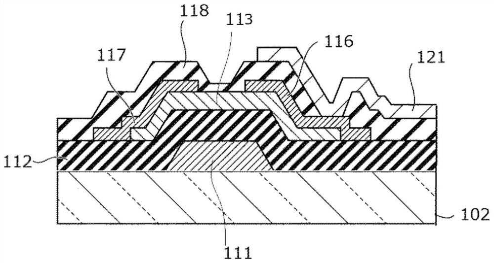
[0275] The configuration of the third embodiment according to the present invention is a liquid crystal display element having a thin film transistor using an oxide semiconductor and a specific liquid crystal composition, preferably on the same substrate as the first substrate on which the electrode layer 3 including the thin film transistor is formed. A color filter 6 is formed on the side. This approach is generally referred to as color filter on array (COA) or the like. Below, use Figure 10 and Figure 11 A specific structure will be described. Figure 10 It is another form of the cross-sectional view obtained by cutting the liquid crystal display element. The composition of the liquid crystal composition is to form the first substrate 2 with alignment layer 4, thin film transistors (11, 13, 15, 16, 17), color filter 6 and pixel electrode 21 on the surface, and the first substrate 2 formed on the surface The second substrate 7 of the alignment layer 4 is spaced apart so ...
PUM
| Property | Measurement | Unit |
|---|---|---|
| temperature | aaaaa | aaaaa |
| electrical resistivity | aaaaa | aaaaa |
| electrical resistivity | aaaaa | aaaaa |
Abstract
Description
Claims
Application Information
 - R&D
- Intellectual Property
- Life Sciences
- Materials
- Tech Scout
- Unparalleled Data Quality
- Higher Quality Content
- 60% Fewer Hallucinations
Browse by: Latest US Patents, China's latest patents, Technical Efficacy Thesaurus, Application Domain, Technology Topic, Popular Technical Reports.
© 2025 PatSnap. All rights reserved.Legal|Privacy policy|Modern Slavery Act Transparency Statement|Sitemap|About US| Contact US: help@patsnap.com


