
Semiconductor light emitting device

A light-emitting device and semiconductor technology, applied in semiconductor devices, electrical components, circuits, etc., can solve the problems of reducing the luminous efficiency of light-emitting devices, and achieve the effect of improving current diffusion effect, increasing luminous efficiency, and preventing current diffusion

Active Publication Date: 2016-06-29
SEOUL VIOSYS CO LTD
View PDF3 Cites 2 Cited by
  • Summary
  • Abstract
  • Description
  • Claims
  • Application Information

AI Technical Summary

Problems solved by technology

[0012] At this time, the injected current is likely to be concentrated around the irregular part of the hole electrode, and this concentration of current inevitably reduces the luminous efficiency of the light-emitting device.

Method used


Image

  • Semiconductor light emitting device
  • Semiconductor light emitting device
  • Semiconductor light emitting device

Examples


Embodiment Construction

[0078] Exemplary embodiments will be described in more detail below with reference to the accompanying drawings. However, the invention may be embodied in different forms and should not be construed as being limited to the embodiments. Rather, these embodiments are provided so that this disclosure will be thorough and complete, and will fully convey the scope of the invention to those skilled in the art. Throughout the invention, the same reference numerals represent the same components in different drawings and different embodiments of the invention.

[0079] Hereinafter, a semiconductor light emitting device and a method of manufacturing the same according to an embodiment of the present invention will be described with reference to the accompanying drawings. In the embodiments of the present invention, a nitride semiconductor will be taken as an example. However, the present invention is not limited thereto.

[0080] A method of manufacturing a nitride semiconductor acco...


PUM

PropertyMeasurementUnit
distanceaaaaaaaaaa
distanceaaaaaaaaaa

Abstract

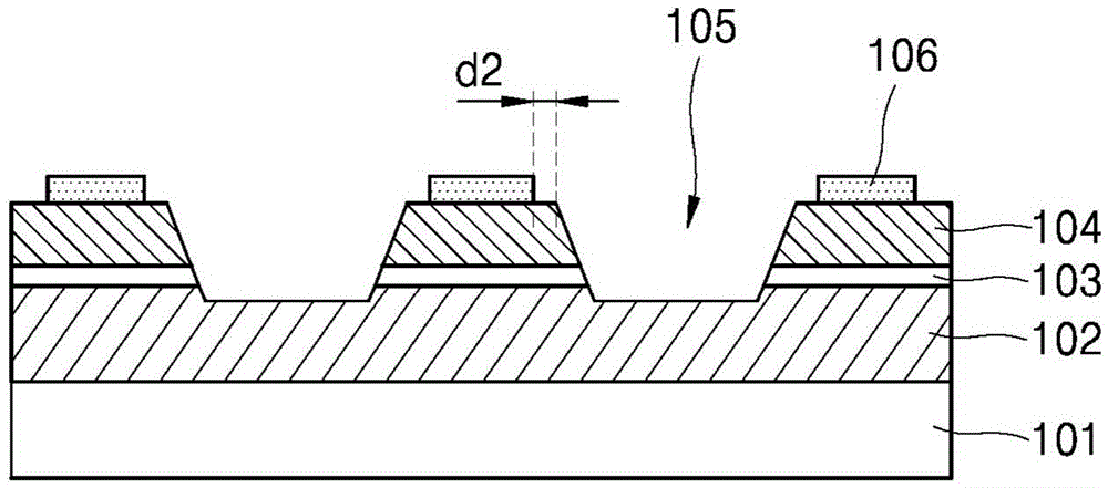
A semiconductor light emitting device may include: a first conductive type nitride semiconductor layer; an active layer formed under the first conductive type nitride semiconductor layer; a second conductive type nitride semiconductor layer formed under the active layer; mesa regions formed upward from the second conductive type nitride semiconductor layer so as to expose the first conductive type nitride semiconductor layer; a second electrode formed under the second conductive type nitride semiconductor layer; a cover metal layer formed at a corner under the second conductive type nitride semiconductor layer so as to overlap a part of the second electrode, and partially exposed in the upward direction; an insulating layer formed under the cover metal layer, the second electrode, and the mesa regions; openings of the insulating layer, formed at portions corresponding to the mesa regions so as to expose the first conductive type nitride semiconductor layer; a first electrode formed under the insulating layer and in the openings; a conductive substrate formed under the first electrode; and a second electrode pad formed over the exposed cover metal layer.

Description

technical field [0001] The present invention relates to a nitride semiconductor light-emitting device, and more particularly, to a semiconductor light-emitting device capable of improving optical efficiency and having a simple structure, a method for preparing the semiconductor light-emitting device, and a light-emitting device including a structure for improving the current diffusion effect . Background technique [0002] A semiconductor light emitting device (such as a nitride semiconductor light emitting device) generally includes a light emitting structure, a first electrode (such as an n-electrode or an n-electrode pad) and a second electrode (such as a p-electrode or a p-electrode pad). The light-emitting structure includes a first conductive type semiconductor layer (such as an n-type semiconductor layer), a second conductive type semiconductor layer (such as a p-type semiconductor layer), and a semiconductor layer between the first conductive type semiconductor layer...

Claims


Application Information

Patent Timeline
Patent Type & Authority Applications(China)
IPC IPC(8): H01L33/38H01L33/40
CPCH01L33/38H01L33/40H01L2933/0016H01L33/20H01L33/22H01L33/382H01L33/0093H01L33/24H01L33/32H01L33/405
Inventor 李美姬李俊熙李所螺张美萝
Owner SEOUL VIOSYS CO LTD
Learn More