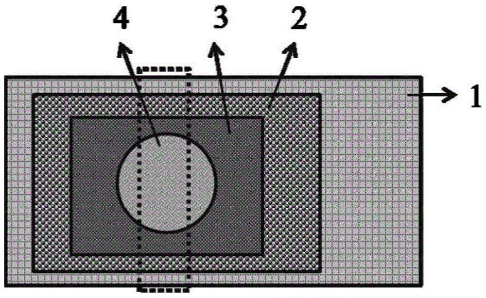
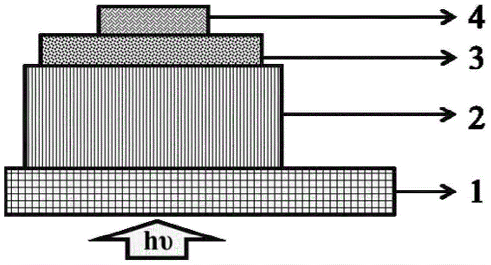
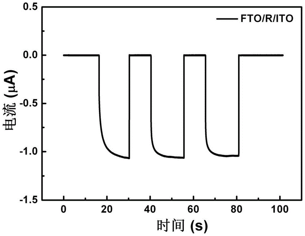
A tio with a built-in electric field 2 Heterogeneous junction ultraviolet/deep ultraviolet detector device and its preparation
A built-in electric field, deep ultraviolet technology, applied in electrical components, semiconductor devices, circuits, etc., to reduce the effect of recombination
- Summary
- Abstract
- Description
- Claims
- Application Information
AI Technical Summary
Problems solved by technology
Method used
Image
Examples
Embodiment 1
[0028] 1) Place the FTO transparent conductive substrate in acetone, isopropanol, ethanol and deionized water for 20 minutes, and then dry it under air flow;
[0029] 2) Place the pre-cleaned FTO transparent conductive substrate (conductive side down) in a polytetrafluoroethylene-lined hydrothermal kettle, add 0.15 mL of tetrabutyl titanate containing HCl and H 2 O volume ratio of 1:1 mixed solution, at 180 ℃ for 2h, grow TiO on the FTO substrate 2 Nanorod array, the length of the nanorod is about 2 μm; as image 3 As shown, the XRD results show that the synthesized nanorod array is a pure rutile phase.
[0030] 3) TiO obtained in step (2) 2 The surface of the rutile phase nanorod array structure is covered with a layer of porous metal mask, which is put into the magnetron sputtering equipment, and the ITO ceramic target is used as the target material. The equipment is first evacuated for 10 -7 Pa, and then pass Ar gas into it, adjust the sputtering pressure to 1Pa, and spu...
Embodiment 2
[0033] 1) Place the FTO transparent conductive substrate in acetone, isopropanol, ethanol and deionized water for 20 minutes, and then dry it under air flow;
[0034] 2) Place the pre-cleaned FTO transparent conductive substrate (conductive side down) in a polytetrafluoroethylene-lined hydrothermal kettle, add 0.15 mL of tetrabutyl titanate containing HCl and H2 O volume ratio of 1:1 mixed solution, at 180 ℃ for 2h, grow TiO on the FTO substrate 2 Rutile phase nanorod array, the length of the nanorod is about 2 μm;
[0035] 3) TiO obtained in step (2) 2 The rutile phase nanorod array is put into the magnetron sputtering equipment, and the metal Ti target is used as the sputtering target. The equipment is first vacuumed to make 10 -7 Pa, and then pass high-purity Ar gas into it, adjust the sputtering pressure to 1Pa, and sputter for 1h under the direct current mode of 100W to obtain a metal Ti layer with a thickness of 200nm. Finally, the obtained bilayer film was heat-treate...
Embodiment 3
[0039] 1) Place the FTO transparent conductive substrate in acetone, isopropanol, ethanol and deionized water for 20 minutes, and then dry it under air flow;
[0040] 2) Place the pre-cleaned FTO transparent conductive substrate (conductive side down) in a polytetrafluoroethylene-lined hydrothermal kettle, add 0.15 mL of tetrabutyl titanate containing HCl and H 2 O volume ratio of 1:1 mixed solution, at 180 ℃ for 2h, grow TiO on the FTO substrate 2 Nanorod array, the length of the nanorod is about 2 μm; as image 3 As shown, the XRD results show that the synthesized nanorod array is a pure rutile phase;
[0041] 3) TiO obtained in step (2) 2 The rutile phase nanorod array is put into the magnetron sputtering equipment, and the metal Ti target is used as the sputtering target. The equipment is first vacuumed to make 10 -7 Pa, then pass into it Ar:O 2 Mixed gas with a volume ratio of 85:15, adjust the sputtering pressure to 1Pa, and sputter for 1h under 400W DC mode to obtai...
PUM
 Abstract
Description
Claims
Application Information
 - Generate Ideas
- Intellectual Property
- Life Sciences
- Materials
- Tech Scout
- Unparalleled Data Quality
- Higher Quality Content
- 60% Fewer Hallucinations
Browse by: Latest US Patents, China's latest patents, Technical Efficacy Thesaurus, Application Domain, Technology Topic, Popular Technical Reports.
© 2025 PatSnap. All rights reserved.Legal|Privacy policy|Modern Slavery Act Transparency Statement|Sitemap|About US| Contact US: help@patsnap.com


