


Quick Research
Generate reliable direction feasibility study reports for your R&D in just a few steps.

Technical Q&A
Discover and master advanced knowledge NOW. Basics, ideas, possibilities, all at once.

Find Solutions
As an expert in R&D theories, this can generate solutions to your technical problems instantly.

Evaluate Feasibility
Analyze your overall solution with one click, know your potential R&D risks in advance.

Monitor Landscape
Get weekly tech updates, stay abreast of the latest tech innovations and key insights.
Interface of optical backboard
A technology of optical backplane and interface, which is applied in the field of optical communication, can solve problems such as complex implementation, and achieve the effects of simple production, small docking loss, and small docking error
- Summary
- Abstract
- Description
- Claims
- Application Information
AI Technical Summary
Problems solved by technology
Method used
Image

Examples
Embodiment 1
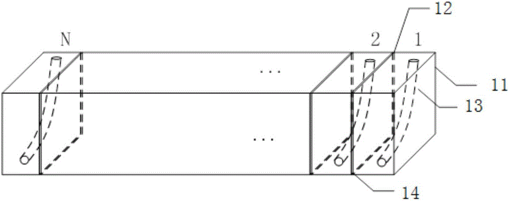
[0025] Such as figure 1 As shown, an optical backplane interface is composed of an array of N multimode optical waveguide chips 1 including a 90° curved optical waveguide 13 , where N≥2. The substrate 12 of each multimode optical waveguide chip is in contact with the upper surface of the adjacent multimode optical waveguide chip (such as figure 1 The adjacent surfaces of the multimode optical waveguide chip 1 and the multimode optical waveguide chip 2, refer to the upper surface 11 of the multimode optical waveguide chip 1) are completely bonded to it by an adhesive 14, and a plurality of multimode optical waveguide chips The bending direction of the inner 90° curved optical waveguide is consistent after bonding. The adhesive is thermosetting adhesive, and the thickness of the adhesive layer is 50um.
[0026] Wherein, the thickness of each multimode optical waveguide chip is equal to the distance between the cores of the optical fiber array minus the thickness of the adhesiv...
Embodiment 2
[0030] An optical backplane interface: including:
[0031] 1. It consists of a 90°bent multimode optical waveguide chip, which can be called a 90°bend waveguide interface. The substrate of each chip and the upper surface of another chip are fully aligned and bonded by UV-curable glue, and then cured by 1wm / cm2 UV light for 5 minutes after bonding. The bending direction of the multimode optical waveguide remains consistent after bonding.
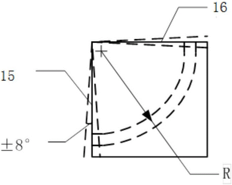
[0032] 2. The array composed of 90°bending multimode optical waveguide chips is optically polished on the waveguide input and output sections, and the polishing angle is 8°. One end of the cross-section is connected to the 200μm core single-port fiber array on the device, and the other end is connected to the single straight waveguide on the optical backplane.
[0033] 3. The thickness of the chip is 400 μm, and the fiber core spacing of the fiber array is 500 μm.
[0034] 4. The bending radius of the 90°bending multimode optical waveguide...
Embodiment 3
[0039] An optical backplane interface, comprising:
[0040] 1. Consisting of 128 90°bent multimode optical waveguide chips, it can be called a 90°bend waveguide interface. The substrate of each chip and the upper surface of another chip are completely aligned and bonded by UV-curable glue, and then cured with heat-curable glue at 200°C for 2 hours after bonding. The bending direction of the multimode optical waveguide remains consistent after bonding.
[0041] 2. The array composed of 90°bending multimode optical waveguide chips is optically polished on the waveguide input and output sections, and the polishing angle is 0°. One end of the section is connected to the 128-port optical fiber array with a 15 μm core on the device, and the other end is connected to the 128-port straight waveguide array on the optical backplane.
[0042] 3. The thickness of the chip is 126.5μm, and the fiber core spacing of the fiber array is 127um.
[0043] 4. The bending radius of the 90°bendin...
PUM
 Abstract
Description
Claims
Application Information
 - R&D Engineer
- R&D Manager
- IP Professional
- Industry Leading Data Capabilities
- Powerful AI technology
- Patent DNA Extraction
Browse by: Latest US Patents, China's latest patents, Technical Efficacy Thesaurus, Application Domain, Technology Topic, Popular Technical Reports.
© 2024 PatSnap. All rights reserved.Legal|Privacy policy|Modern Slavery Act Transparency Statement|Sitemap|About US| Contact US: help@patsnap.com