
A kind of mask set for etching and substrate etching method using the same

A mask group and substrate technology, applied in the field of microelectronics, can solve the problems of fast lateral shrinkage, straight sidewall modification, poor etching resistance of photoresist masks, etc. Lateral shrinkage speed, the effect of reducing corners

Active Publication Date: 2018-07-06
BEIJING NAURA MICROELECTRONICS EQUIP CO LTD
View PDF4 Cites 0 Cited by
  • Summary
  • Abstract
  • Description
  • Claims
  • Application Information

AI Technical Summary

Problems solved by technology

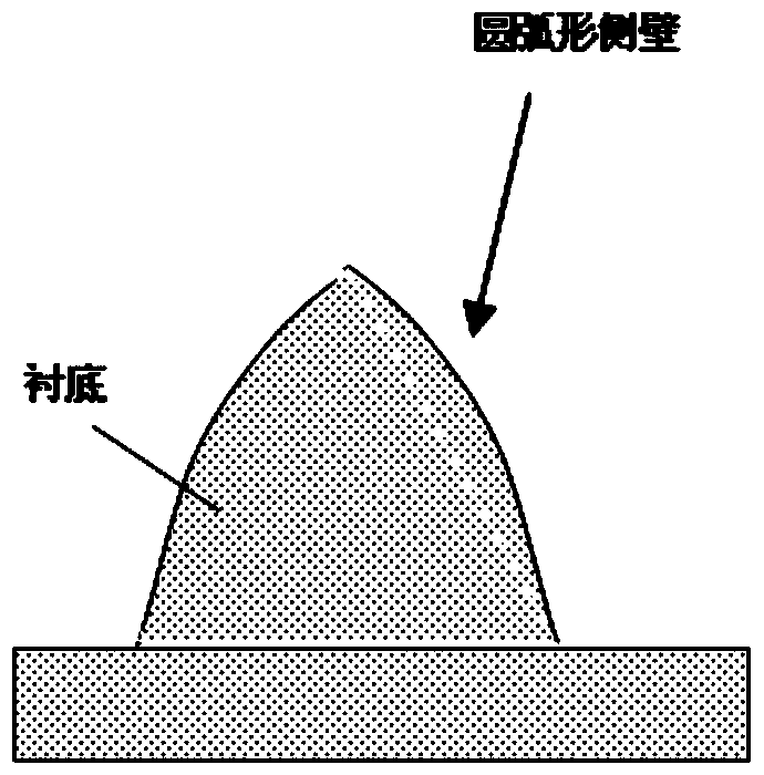
However, due to the poor etch resistance of the photoresist mask, its lateral shrinkage speed is too fast, resulting in a small inclination angle C of the sidewall top 2, that is, the corners on the substrate sidewall (sidewall bottom 1 and The included angle of the top 2 of the sidewall) is too large, so that the over-etching step cannot modify the sidewall straight, and the finally obtained graphic appearance is that the sidewall forms an arc shape that is insufficiently modified, such as figure 2 shown

Method used


Image

  • A kind of mask set for etching and substrate etching method using the same
  • A kind of mask set for etching and substrate etching method using the same
  • A kind of mask set for etching and substrate etching method using the same

Examples


Embodiment Construction

[0024] In order for those skilled in the art to better understand the technical solution of the present invention, the etching mask set provided by the present invention and the substrate etching method using it will be described in detail below with reference to the accompanying drawings.

[0025] First of all, it should be noted that the etching mask set provided by the present invention is to form the required pattern on the surface of the substrate by using two photolithography processes. A mask set for etching is used, and then a required pattern is carved out of the mask set for etching by using a photolithography process.

[0026] image 3 Two views of the cross-section and top view of the mask set for etching provided by the embodiment of the present invention. see image 3 , the mask set for etching includes a first mask layer 11 and a second mask layer 12, which are arranged sequentially from the surface of the substrate 10 from bottom to top, that is, the first ma...


PUM


Abstract

The etching mask set provided by the present invention and the substrate etching method using the same include the first mask layer made of photoresist material, and the material that can improve the etching selectivity ratio relative to the substrate making a second mask layer, wherein the first mask layer is disposed on the surface of the substrate; the second mask layer is disposed on the first mask layer; the respective patterns of the first mask layer and the second mask layer The width of the bottom is set such that: the inclination angle of the preset connection line between the first mask layer and the second mask layer is consistent with the fixed inclination angle of the first mask layer. The mask set for etching provided by the present invention can achieve the purpose of improving the figure topography of the substrate.

Description

technical field [0001] The invention relates to the technical field of microelectronics, in particular to an etching mask set and a substrate etching method using the same. Background technique [0002] PSS (Patterned Sapp Substrates, patterned sapphire substrate) technology is a method commonly used at present to improve the light extraction efficiency of GaN (gallium nitride)-based LED devices. During the PSS process, it usually grows a mask for dry etching on the substrate, and uses a photolithography process to carve the mask into a pattern; then uses ICP technology to etch the surface of the substrate to form the required pattern , and then remove the mask, and use the epitaxial process to grow a GaN film on the etched substrate surface. At present, because the graphic morphology obtained by etching the substrate surface with ICP technology can affect the light extraction effect of LED devices, especially the conical graphic morphology with straight side walls can sign...

Claims


Application Information

Patent Timeline
Patent Type & Authority Patents(China)
IPC IPC(8): H01L21/02H01L21/027
Inventor 李宗兴
Owner BEIJING NAURA MICROELECTRONICS EQUIP CO LTD
Learn More