Multi-camera module and assembling method therefor

A multi-camera and assembly method technology, applied in radiation control devices, semiconductor/solid-state device components, semiconductor devices, etc., can solve the problems of difficult dust control, difficult manufacturing reliability, and poor image imaging quality, etc. Achieve the effect of improving the assembly accuracy and module performance, the assembly method is simple and easy, and the gold wire extension performance is good.

Pending Publication Date: 2016-06-01
GALAXYCORE SHANGHAI
View PDF5 Cites 4 Cited by
  • Summary
  • Abstract
  • Description
  • Claims
  • Application Information

AI Technical Summary

Problems solved by technology

However, CSP packaging has the following obvious problems: 1 affects product performance: the absorption, refraction, reflection and scattering of light by thick support glass have a great impact on the performance of image sensors, especially small pixel size products; 2 reliability issues : The thermal expansion coefficient difference between the components in the package structure and the sealing gas in the cavity have reliability problems in the subsequent SMT process or changes in the product use environment; 3 Large investment scale, large environmental pollution control requirements, and long production cycle , the unit chip cost is high, especially for high-pixel and large-size image sensor products
However, COB packaging has the following obvious problems: 1. Dust control is very difficult, requiring ultra-high clean room levels, and high manufacturing maintenance costs; 2. Product design customization, long cycle, and insufficient flexibility; 3. It is not easy to scale production ;
However, the FC package has the following obvious problems: 1. The package has high requirements on the PCB substrate, and has a similar thermal expansion coefficient to Si, and the cost is very high; 2. Manufacturing reliability is very difficult, and the connection between all the bumps and pads of the thermosonic is consistent. The performance requirements are very high, the bumps and pads are hard-connected, and the ductility is not good; 3. The dust control is difficult, the process environment requirements are high, and the cost is high;
[0010] This method of assembling the camera module has the following disadvantages: For the camera module, it is necessary to use high-precision installation equipment to carry out the precise installation of the above step 3, otherwise it will affect the imaging effect of the camera module, and then assembled The qualified rate of finished products of camera modules is not high; especially for high-pixel camera modules, it is difficult to complete the precise installation of the above step 3 with ordinary installation equipment, so that the imaging effect of high-pixel camera modules is affected. Large impact, the imaging quality of the formed image is poor, especially the imaging quality around the image is obviously bad
[0013] In addition, with the rapid development of consumer electronic products, the single camera suitable for portable electronic devices already has defects in some market segments, and the focusing ability and dynamic balance are difficult to meet the needs under certain circumstances.
Multi-camera modules have appeared in portable electronic devices. Multi-camera modules have been used in the main camera of smartphones. However, in the assembly of multi-camera modules, there will be misalignment of the photosensitive surfaces of the image sensor chips, with height and deviation angles. The problem will bring unsolvable problems in the subsequent imaging process

Method used


Image

  • Multi-camera module and assembling method therefor
  • Multi-camera module and assembling method therefor
  • Multi-camera module and assembling method therefor

Examples


Embodiment Construction

[0041] In the following detailed description of the preferred embodiment, reference is made to the accompanying drawings which form a part hereof. The accompanying drawings show, by way of example, specific embodiments in which the invention can be practiced. The illustrated embodiments are not intended to be exhaustive of all embodiments in accordance with the invention. It is to be understood that other embodiments may be utilized and structural or logical changes may be made without departing from the scope of the present invention. Accordingly, the following detailed description is not limiting, and the scope of the invention is defined by the appended claims.

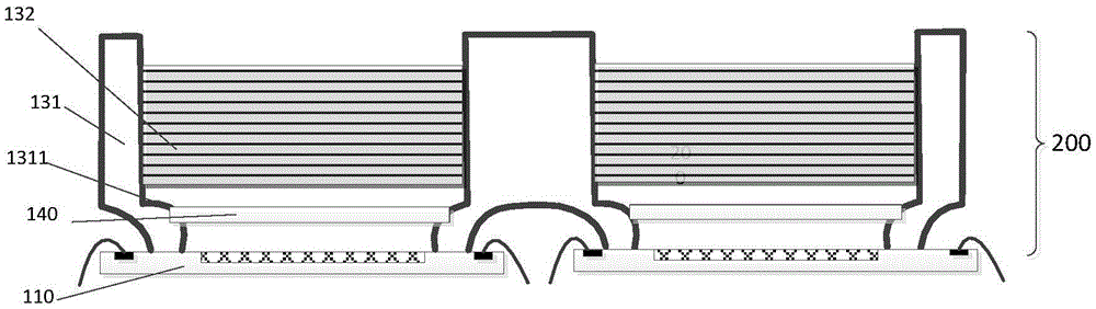
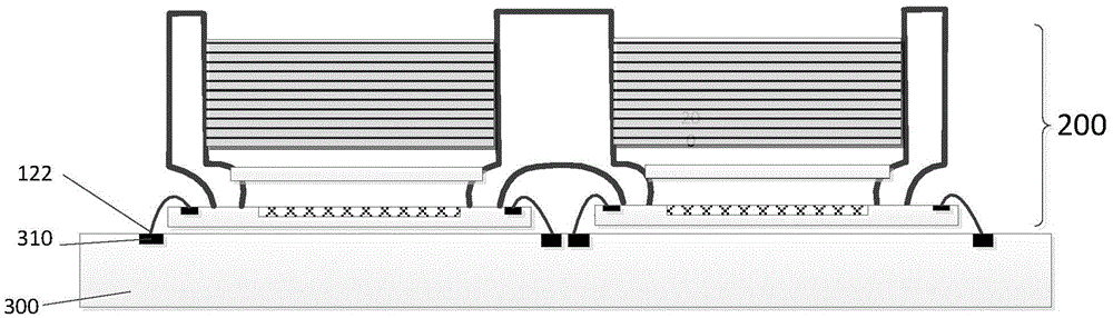
[0042] In order to illustrate the packaging method of the present invention more clearly, in the following embodiments, glass is used as the substrate. Those skilled in the art can understand that the substrate can also be made of other transparent materials.

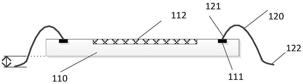
[0043] figure 1 is a schematic diagram of an image...


PUM


Abstract

The invention provides an assembling method for a multi-camera module. The assembling method comprises the steps of providing multiple image sensor chips with suspending metal wires, wherein the first end of each metal wire is arranged on a bonding pad of each image sensor chip in a bonding manner, while the second end of each metal wire is suspended on each image sensor chip; providing a lens cone framework, wherein the lens cone framework adopts an integral structure and is suitable for assembling multiple groups of lens modules and the multiple image sensor chips; and assembling the multiple image sensor chips and the lens cone framework into standard components, and assembling the standard components and circuit boards into the multi-camera module through the second ends of the metal wires.

Description

technical field [0001] The invention relates to the field of semiconductor manufacturing, in particular to an assembly method of a multi-camera module. Background technique [0002] At present, the mainstream image sensor (CIS: CMOSImageSensor) packaging methods include: chip-scale packaging (ChipScalePackage, CSP), board-integrated packaging (ChipOnBoard, COB) and flip-chip packaging (FlipChip, FC). [0003] CISCSP is a packaging technology commonly used in low-end and low-pixel (2M pixels or below) image sensors at present, and can adopt Dielevel (chip level) or Waferlevel (wafer level) packaging technology. This packaging technology usually uses wafer-level glass and wafer bonding and uses cofferdams to separate the image sensor chips of the wafer, and then makes pad surface or pad in-plane holes in the pad area of ​​the polished wafer. Through-silicon via technology (TSV: ThroughSiliconVia) with side ring metal connection or T-shaped metal contact chip size packaging te...

Claims


Application Information

Patent Timeline
Patent Type & Authority Applications(China)
IPC IPC(8): H01L27/146H01L21/60H01L23/488
CPCH01L24/80H01L27/146H01L27/14601H01L27/14683H01L23/488H01L2224/02H01L2224/80H01L2224/48091H01L2224/48137H01L2224/73265H01L2924/00014
Inventor 赵立新侯欣楠
Owner GALAXYCORE SHANGHAI
Why Eureka
Try Eureka