An input undervoltage protection circuit and method
A technology for input undervoltage and circuit protection, applied to electrical components, output power conversion devices, etc., can solve problems such as restarting and unstable product output, and achieve the effect of preventing malfunctions
- Summary
- Abstract
- Description
- Claims
- Application Information
AI Technical Summary
Problems solved by technology
Method used
Image
Examples
Embodiment 1
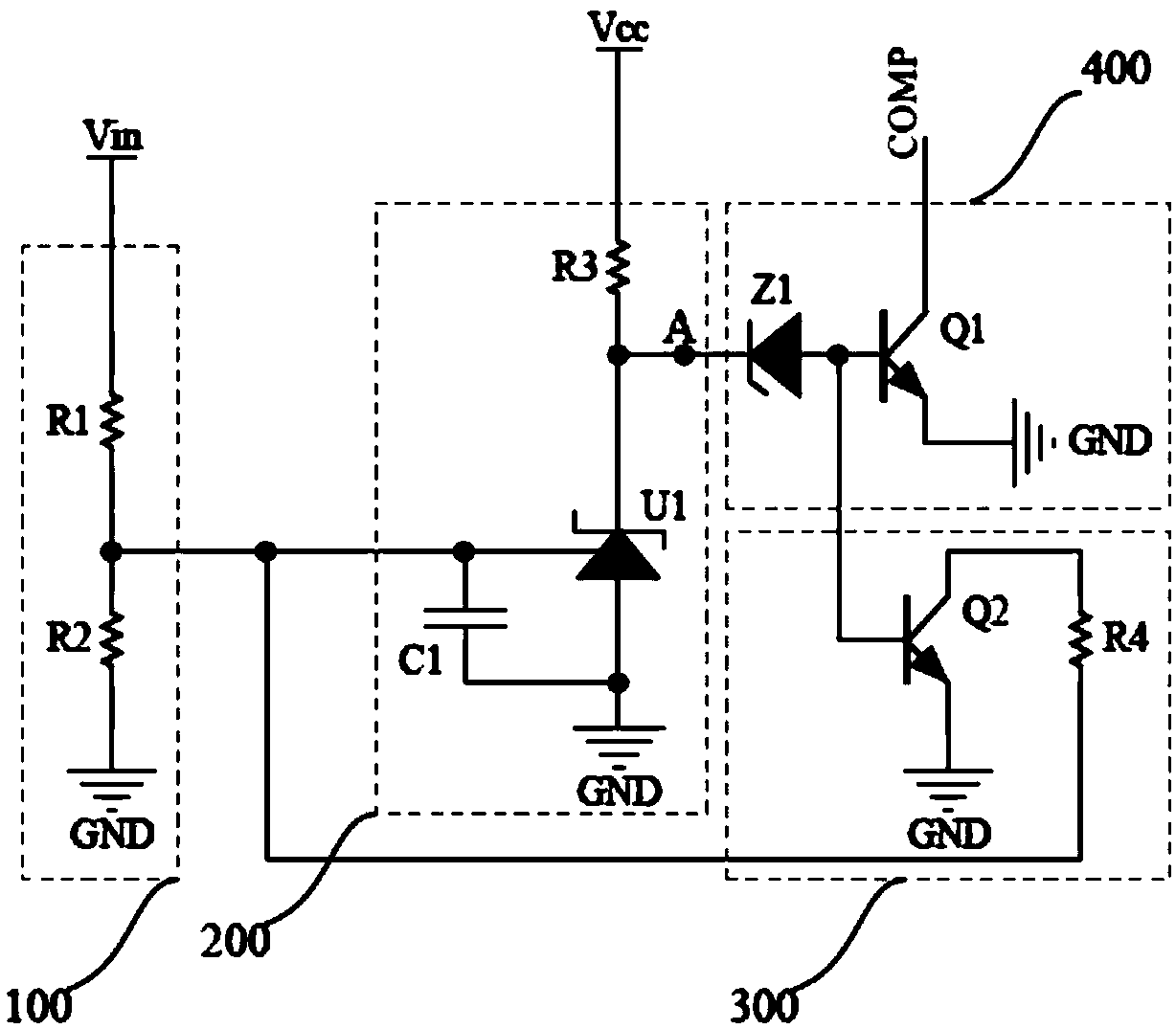
[0052] Figure 4 It is the schematic circuit diagram of the first embodiment of the present invention. The sampling circuit 100 includes: a resistor R1 and a resistor R2; The output of the connection point of the above-mentioned resistor R2 is the above-mentioned sampling signal. The control circuit 200 includes: capacitor C1, error amplifier TL431 ( Figure 4 U1) and resistor R5; switching power supply control IC ( Figure 5 The Vcc pin of U2) is grounded sequentially through the resistor R5, the cathode of the error amplifier TL431, and the anode of the error amplifier TL431; the capacitor C1 is connected in parallel to the error amplifier TL431 Between the anode and the reference pin; the reference pin of the error amplifier TL431 receives the sampling signal; the cathode of the error amplifier TL431 outputs the control signal; the reference pin of the error amplifier TL431 is the The input terminal of the control circuit described above. The hysteresis circuit 300 incl...
Embodiment 2
[0062] Figure 7 It is the schematic circuit diagram of the second embodiment of the present invention, Figure 8 It is the schematic diagram of the circuit applied in the DC-C switching power supply of the second embodiment of the present invention. The difference between the second embodiment and the first embodiment is that it also includes a diode D1 and a diode D2, and the anode of the diode D1 is connected to the The resistor R6, the cathode of the diode D1 is connected to the collector of the transistor Q1. The anode of the diode D2 is connected to the control terminal of the Vcc pin regulator circuit of the switching power supply control IC, and the cathode of the diode D2 is connected to the cathode of the diode D1.
[0063] The voltage stabilizing circuit above is a voltage stabilizing circuit between the Vcc pin of the switching power supply control IC and the auxiliary winding, and is generally composed of a triode and a voltage stabilizing diode, such as Figure...
Embodiment 3
[0066] Figure 9 It is the schematic circuit diagram of the third embodiment of the present invention, Figure 10It is the schematic diagram of the circuit applied in the DC-C switching power supply of the third embodiment of the present invention. The difference between the third embodiment and the second embodiment is that it also includes a Zener diode D3, and the anode of the Zener diode D3 The collector and cathode of the transistor Q1 are connected to the cathode of the diode D1. When the transistor Q1 is turned on, the regulator tube D3 maintains the level of the Vcc pin of the control IC at an appropriate value to ensure that the hysteresis circuit 300 is in a working state and avoid small-scale fluctuations in the input voltage after the product input undervoltage occurs the product restarts.
PUM
 Abstract
Description
Claims
Application Information
 - Generate Ideas
- Intellectual Property
- Life Sciences
- Materials
- Tech Scout
- Unparalleled Data Quality
- Higher Quality Content
- 60% Fewer Hallucinations
Browse by: Latest US Patents, China's latest patents, Technical Efficacy Thesaurus, Application Domain, Technology Topic, Popular Technical Reports.
© 2025 PatSnap. All rights reserved.Legal|Privacy policy|Modern Slavery Act Transparency Statement|Sitemap|About US| Contact US: help@patsnap.com


